Circuit and method for test and repair

a technology of circuits and circuits, applied in the field of test and repair of memory, can solve problems such as error detection and repair schemes, cell failure to properly store data, and raise problems

a technology of circuits and circuits, applied in the field of test and repair of memory, can solve problems such as error detection and repair schemes, cell failure to properly store data, and raise problems

US6904552B2Inactive Publication Date: 2005-06-07MICRON TECH INC

Image

  • Circuit and method for test and repair
  • Circuit and method for test and repair
  • Circuit and method for test and repair

Examples


Embodiment Construction

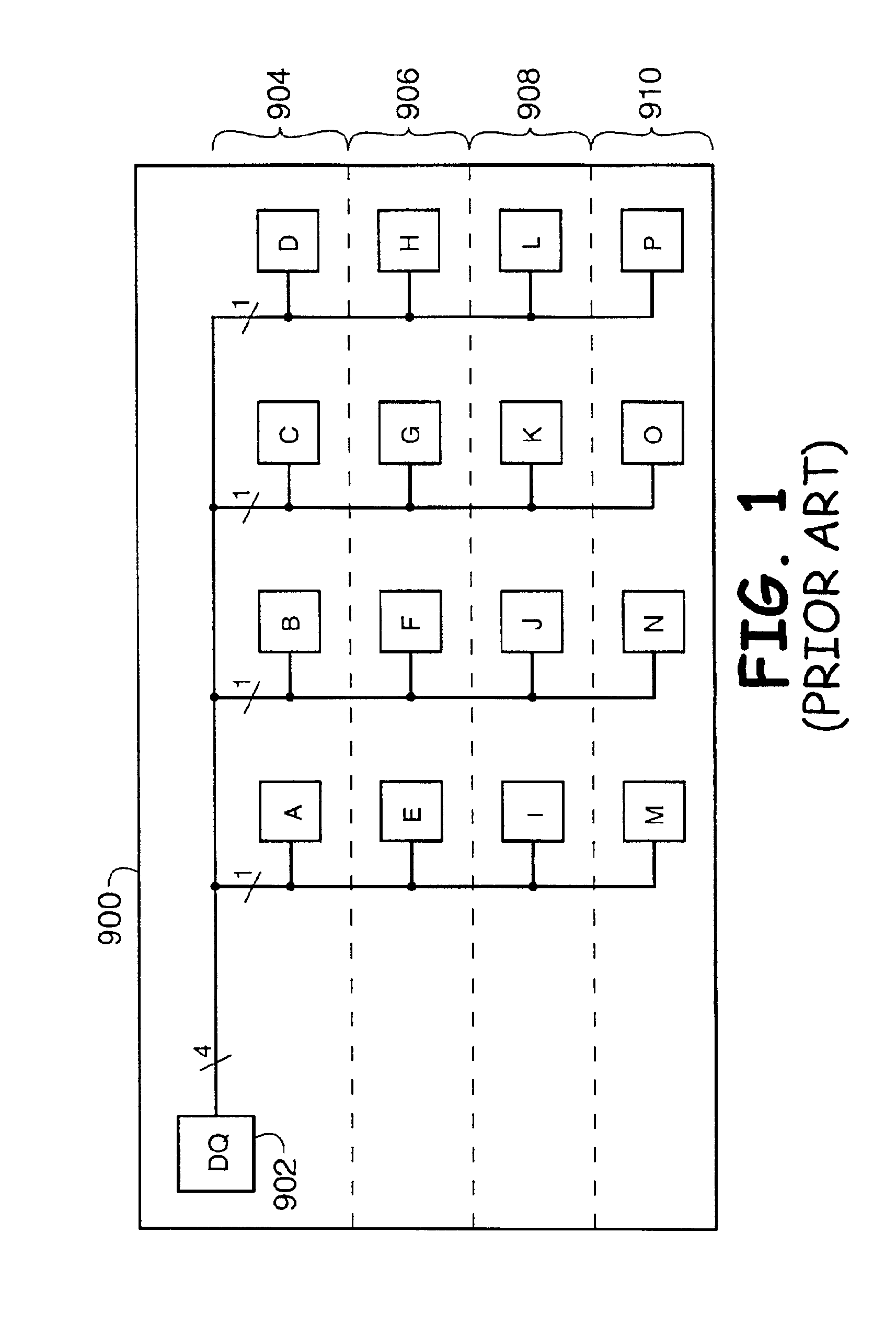
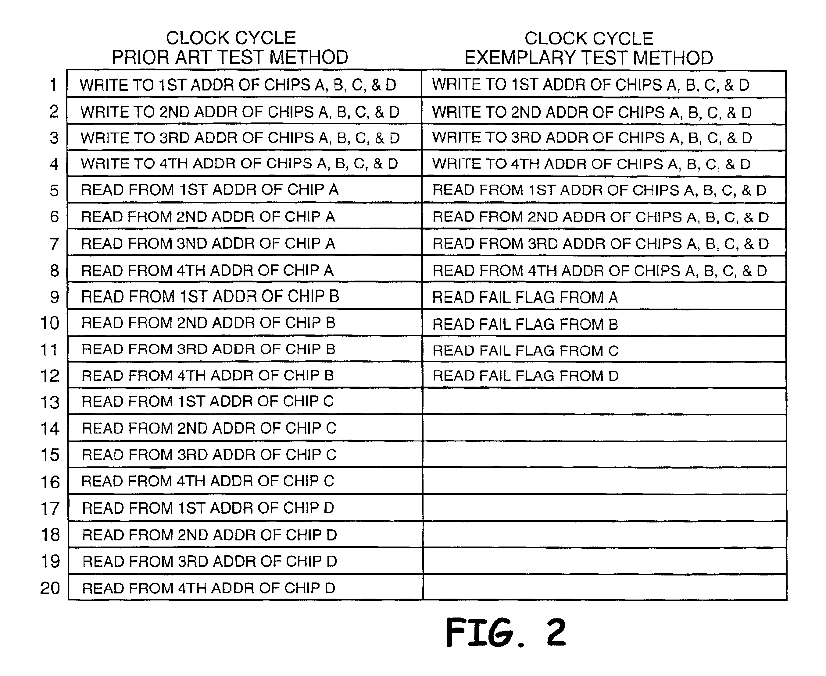
[0015]In terms of error detection, exemplary embodiments of the current invention shorten test time by presenting a testing scheme alternative to the one presented in the Background. To begin with, a simplified test method practiced in the prior art is presented. FIG. 1 presents a portion of a simplified tester 900 having only four DQ's 902. While the tester 900 may be able to physically hold 16 chips (A-P), its circuitry is designed to direct signals to and from at most four chips at one time. It is understood that the tester 900 also has conductive lines (not shown) that carry address and command information to the chips, and that these lines are also limited in number and so can direct signals to and from at most four chips at a time. The areas in which the tester may communicate in such a fashion are identified in this specification as “regions.” Tester 900 has four regions 904, 906, 908, and 910. Further, it is assumed for purposes of explanation that the parts A-P are “×1” par...


PUM


Abstract

A preferred exemplary embodiment of the current invention concerns a memory testing process, wherein circuitry is provided on a chip to allow on-chip comparison of stored data and expected data. The on-chip comparison allows the tester to transmit in a parallel manner the expected data to a plurality of chips. In a preferred embodiment, at most one address—and only the column address—corresponding to a failed memory cell is stored in an on-chip register at one time, with each earlier failed addresses being cleared from the register in favor of a subsequent failed address. Another bit—the “fail flag” bit—is stored in the register to indicate that a failure has occurred. If the fail flag is present in a chip, that chip is repaired by electrically associating the column address with redundant memory cells rather than the original memory cells. Subsequently, the chip's register may be cleared and testing may continue. It is preferred that the register and related logic circuitry be configured to avoid storing an address that is already associated with a redundant cell, even though that redundant cell has failed.

Description

TECHNICAL FIELD[0001]The present invention relates generally to the computer memory field and, more specifically, to test and repair of memory.BACKGROUND OF THE INVENTION[0002]A memory device is often produced using a semiconductor fabrication process. In the current application, the term “semiconductor” will be understood to mean any semiconductor material, including but not limited to bulk semiconductive materials (either alone or in assemblies comprising other materials thereon), and semiconductive material layers (either alone or in assemblies comprising other materials). Moreover, it shall be understood that a semiconductor device may comprise conductive and insulative materials as well as a semiconductive material. The result of a semiconductor process may be a die comprising memory circuitry, and it may be desirable to test that circuitry at some point during the process of constructing a memory device comprising that die. For instance, testing may occur while the die is part...

Claims


Application Information

Patent Timeline
07 Jun 2005
Publication
US6904552B2
IPC
G11C29/00; G11C29/04; G11C29/44; G01R31/28; G11C11/401; G11C11/413; G11C16/02; G11C29/12
CPC
G11C29/72; G11C29/44; G11C29/00
Inventors
COWLES, TIMOTHY B.