

Method of driving plasma display panel and apparatus thereof
a plasma display and display panel technology, applied in the direction of instruments, static indicating devices, etc., can solve the problems of difficult to reduce the voltage applied to the address electrode, and the difficulty of reducing the data voltag
- Summary
- Abstract
- Description
- Claims
- Application Information
AI Technical Summary
Benefits of technology
Problems solved by technology
Method used
Image

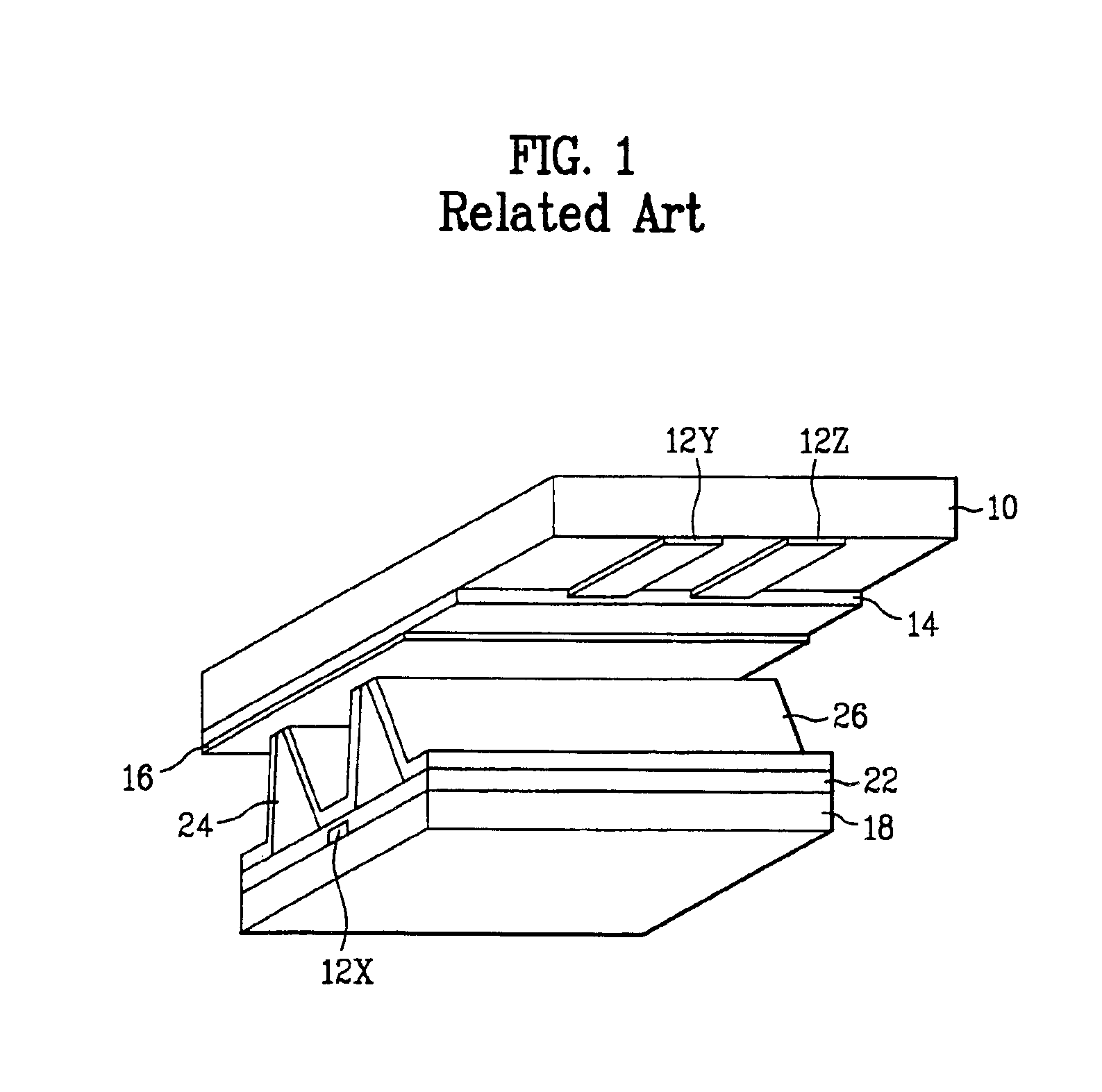
Examples
first embodiment
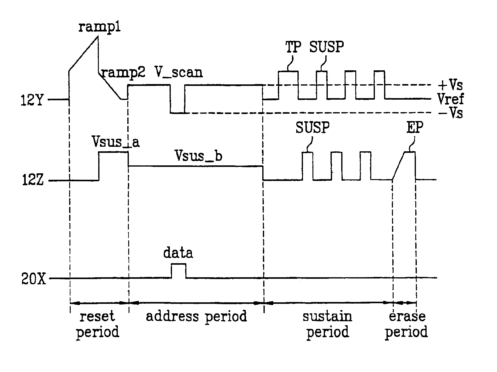
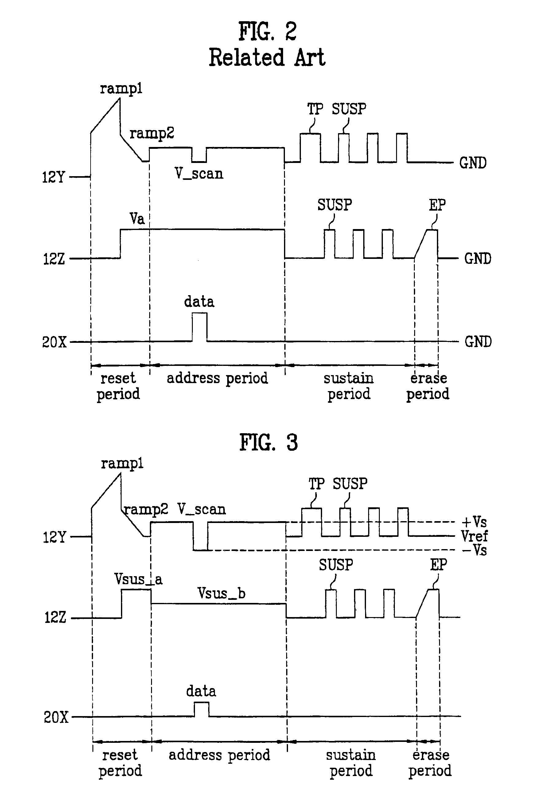
[0055]FIG. 3 illustrates a graph of driving waveforms applied to the respective electrodes for a PDP driving according to the present invention, FIG. 4 illustrates a diagram of a driving circuit of a scan electrode for a PDP driving according to the present invention, and FIG. 5 illustrates a timing diagram of generating waveforms of a scan electrode according to the present invention.
[0056]The present invention relates to a driving system of PDP equipped with at least three electrodes (scan electrode, sustain electrode, address electrode), in which a driving time for expressing a specific gray scale of a single frame in a 3-electrodes AC surface discharge type PDP is divided into a plurality of sub-fields.
[0057]And, each of the sub-fields is divided again into a rest period, an address period, and a sustain period for time.
[0058]In a general PDP driving, pulses of which count is determined by each of the periods of the respective sub-fields are applied to the respective electrodes ...
second embodiment
[0116]FIG. 6 illustrates a graph of driving waveforms applied to the respective electrodes for a PDP driving according to the present invention.
[0117]Referring to FIG. 6, a PDP driving according to a second embodiment of the present invention is mainly divided into a reset period initializing cells so as to equalize initial conditions of entire discharge cells, an address period selecting a discharge cell, a sustain period expressing a gray scale according to a discharge count, and an erase period erasing the discharge.
[0118]The reset period is divided into set-up and set-down periods. And, the drive of the set-up and set-down periods is explained in the foregoing description. Hereinafter, explanation for the reset period is skipped.
[0119]In the address period following the address period, centering on the reference potential Vref of the reset and sustain discharges, the scan electrode 12Y is supplied with a pulse of the scan voltage Vscan swinging between the positive voltage +Vs h...
PUM
 Abstract
Description
Claims
Application Information