Micro-mirror element

a technology of mirror elements and micro-mirror arrays, applied in the direction of optical elements, acceleration measurement using interia forces, instruments, etc., can solve the problems of increasing the size of the substrate or the micro-mirror array, increasing the difficulty of forming the mirror surfaces and the wiring on the same substrate,

Active Publication Date: 2005-06-14
FUJITSU LTD
View PDF13 Cites 102 Cited by
  • Summary
  • Abstract
  • Description
  • Claims
  • Application Information

AI Technical Summary

Benefits of technology

[0012]The present invention has been proposed under the circumstances described above. It is therefore an object of the present invention t

Problems solved by technology

This poses a problem of increased size of the substrate or the micro-mirror array.
In addition, increase in the number of

Method used


Image

  • Micro-mirror element
  • Micro-mirror element
  • Micro-mirror element

Examples


first embodiment

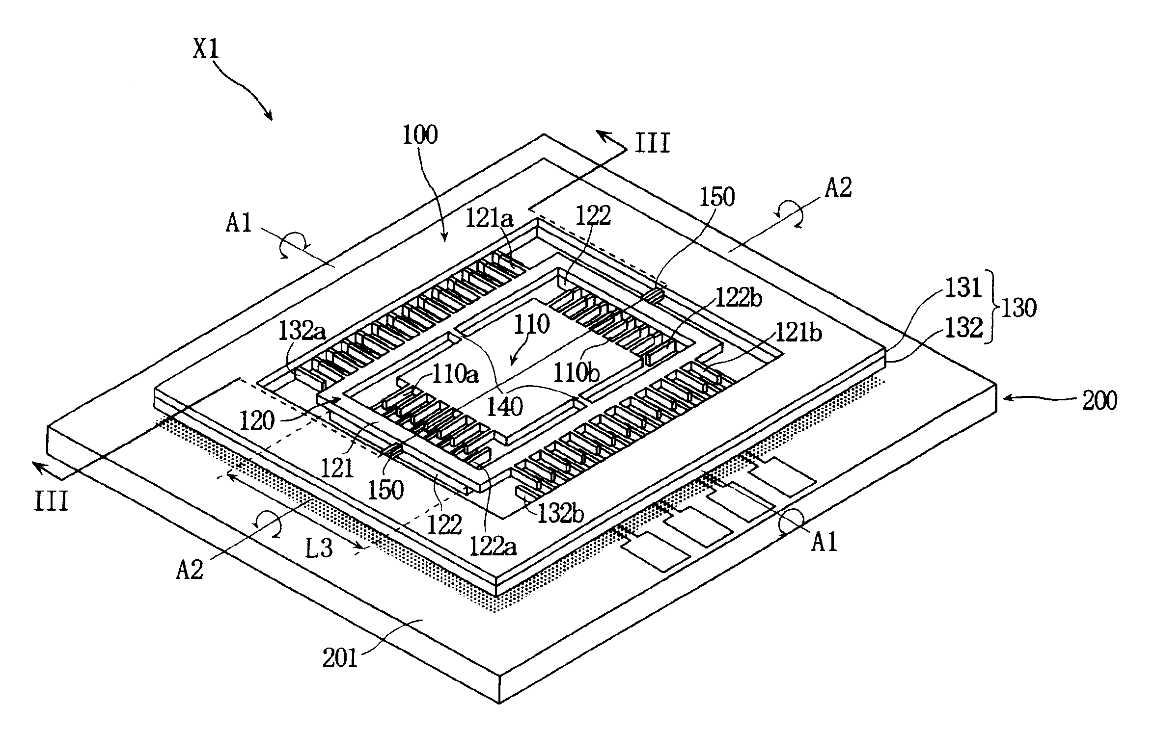
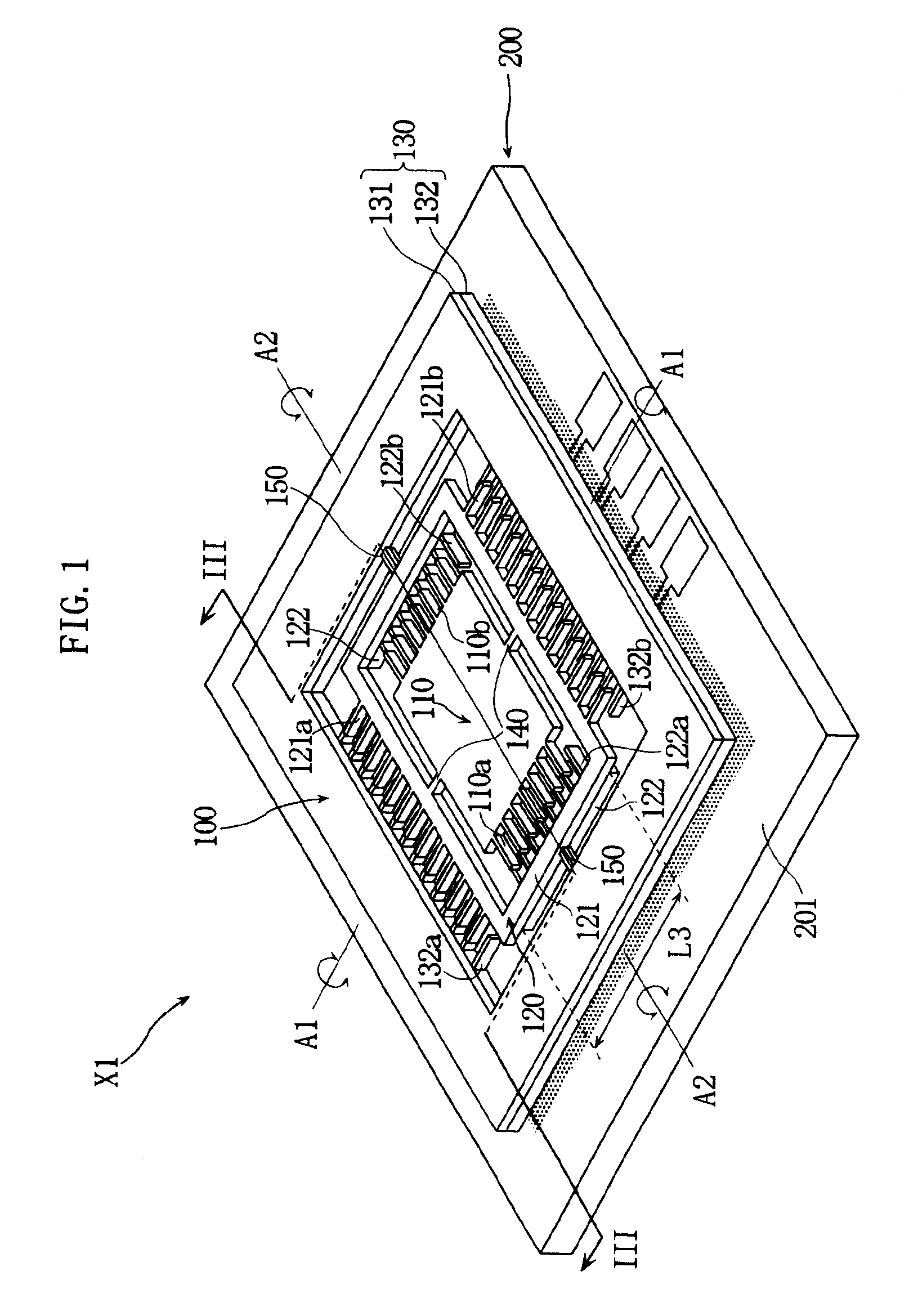
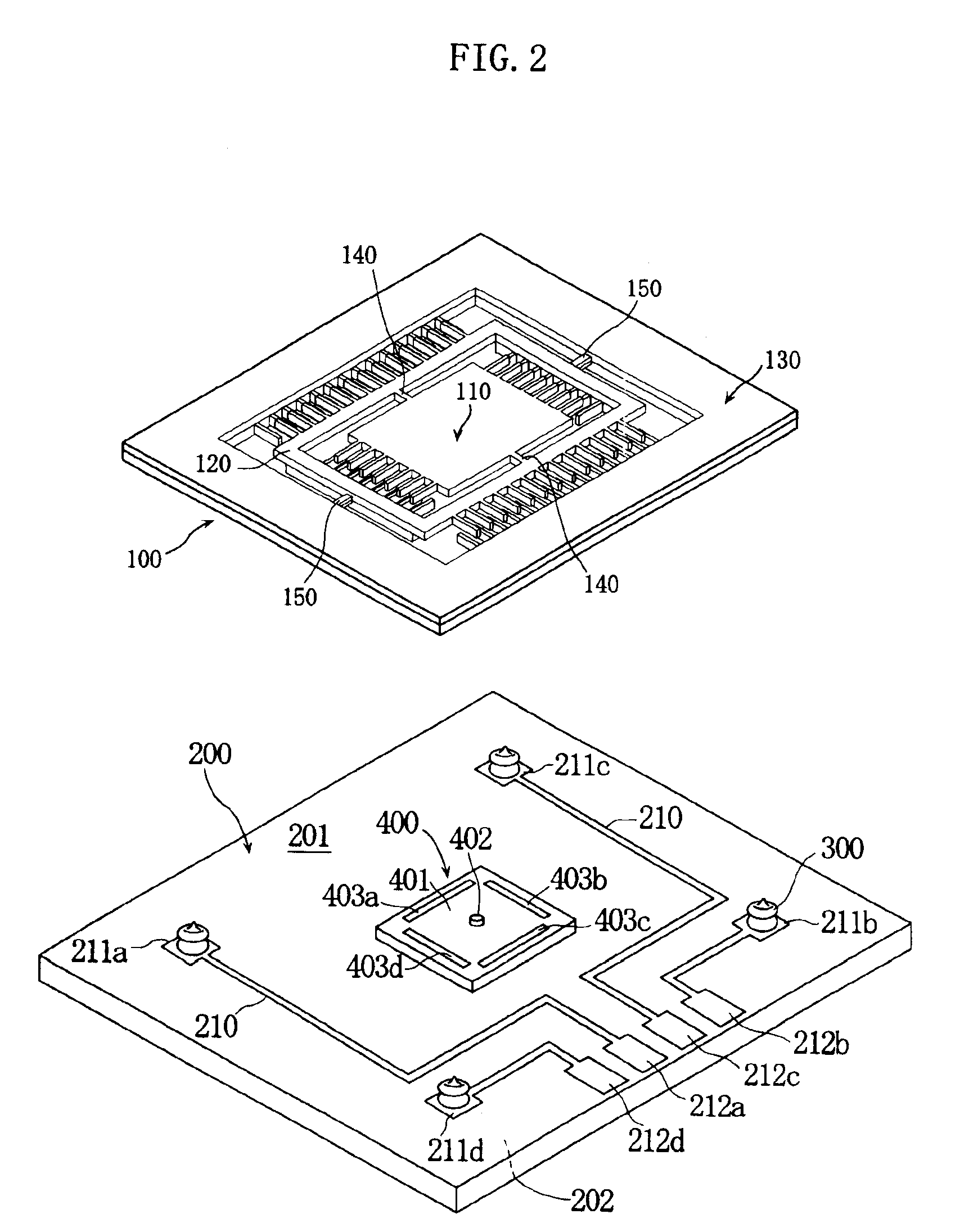
[0032]FIG. 1 is a perspective view showing a micro-mirror element X1 according to the present invention. FIG. 2 is an exploded perspective view of the micro-mirror element X1 in FIG. 1. FIG. 3 is a sectional view taken along lines III—III in FIG. 1.

[0033]The micro-mirror element X1 includes a micro-mirror substrate 100, a wiring substrate 200, electroconductive spacers 300 disposed between the two substrates, and an optical sensor unit 400. The micro-mirror substrate 100 has a mirror-formed portion 110, an inner frame 120 surrounding the portion 110, an outer frame 130 surrounding the inner frame 120, a pair of torsion bars 140 connecting the mirror-formed portion 110 to the inner frame 120, and a pair of torsion bars 150 connecting the inner frame 120 to the outer frame 130. The torsion bars 140 define a pivotal axis A1 for the mirror-formed portion 110 to pivot with respect to the inner frame 120. The torsion bars 150 define a pivotal axis A2 for the inner frame 120 and the mirror...

second embodiment

[0049]FIG. 5 is a perspective view of a micro-mirror element X2 according to the present invention. FIG. 6 is an exploded perspective view of the micro-mirror element X2. FIG. 7 is a partial sectional view showing the structure of the micro-mirror element X2.

[0050]The micro-mirror element X2 of the second embodiment includes a micro-mirror substrate 100, a wiring substrate200, conductive spacers 300 between the two, and a plurality of optical sensor units 400 (nine units by the illustrated example). The micro-mirror substrate 100 includes a plurality of micro-mirror units X2′ (nine units in the illustrated example) and a common outer frame 130′ surrounding the units X2′. Each of the micro-mirror units X2′ includes a mirror-formed portion 110, an inner frame 120 surrounding the portion 110, a pair of torsion bars 140 connecting the mirror-formed portion 110 and the inner frame 120, and a pair of torsion bars 150 connecting the inner frame 120 and the common outer frame 130′. The mirr...


PUM


Abstract

A micro-mirror element includes a micro-mirror substrate, a wiring substrate and an electroconductive spacer disposed between the two substrates. The micro-mirror substrate is formed integral with a frame, a moving portion having a mirror portion, and a torsion bar connecting the frame to the moving portion. The wiring substrate is provided with a wiring pattern. The electroconductive spacer separates the micro-mirror substrate from the wiring substrate and also electrically connects the frame to the wiring pattern. The wiring substrate has a surface that faces the micro-mirror substrate. A detector is provided on this surface for detecting the pivot angle of the mirror portion.

Description

BACKGROUND OF THE INVENTION[0001]1. Field of the Invention[0002]The present invention relates to a micro-mirror element to be incorporated in e.g. an optical switching device which switches optical paths between a plurality of optical fibers by changing the direction of light reflection.[0003]2. Description of the Related Art[0004]In recent years, optical communications technology is utilized widely in a variety of fields. In the optical communications, optical fibers serve as a medium through which optical signals are passed. For switching the optical signal passing through a given optical fiber to another fiber, so-called optical switching devices are often used. In order to achieve high quality optical communications, the optical switching device needs to have such characteristics as high capacity, high speed and high reliability in switching action. In view of these, micro-mirror elements manufactured by utilizing a micro-machining technology are attracting attention as a switch...

Claims


Application Information

Patent Timeline
IPC IPC(8): G02B26/08B81B3/00B81B7/00
CPCB81B7/0006G02B26/0841B81B2201/042B81B3/0083
Inventor MI, XIAOYUSONEDA, HIROMITSUUEDA, SATOSHISAWAKI, IPPEI
Owner FUJITSU LTD
Why Eureka
Try Eureka