Method of fabricating polysilicon film

a technology of polysilicon and film, applied in the direction of semiconductor devices, electrical apparatus, transistors, etc., can solve the problems of adversely affecting the crystallization of thin films, and achieve the effect of increasing the silicon grain siz

Inactive Publication Date: 2005-07-12
AU OPTRONICS CORP
View PDF2 Cites 57 Cited by
  • Summary
  • Abstract
  • Description
  • Claims
  • Application Information

AI Technical Summary

Benefits of technology

[0016]Accordingly, in the light of the foregoing, one object of the present invention is to provide a method of forming polysilicon film, which method is capable of increasing the lateral temperature gradient between portions of the amorphous silicon layer in order to induce lateral crystallization of polysilicon grains. Therefore a polysilicon film having larger grain size can be formed.
[0017]Another object of the invention is to provide a method of forming polysilicon film, which method is capable of increasing the lateral temperature gradient between prescribed regions of the amorphous silicon layer in order to induce crystallization of amorphous silicon layer at specific locations to increase the silicon grain size. Therefore, prescribed regions having larger silicon grain size can be formed.
[0018]In accordance with the above objects and other advantages, as broadly embodied and described herein, the present invention provides a method of forming polysilicon film comprising the steps of: forming an amorphous silicon layer on a substrate; forming a first optical layer on the amorphous silicon layer, wherein the first optical layer is comprised of a first region with a first thickness and a second region with a second thickness, and a reflectivity of the first region is higher than a reflectivity of the second region; performing a laser annealing process wherein a temperature of the amorphous silicon layer beneath the first region is lower than that of the amorphous silicon layer beneath the second region so that the amorphous layer beneath the first region is partially or not completely melted and the amorphous silicon, layer beneath the second region is substantially or completely melted; and crystallizing the melted silicon layer. Because of the differential lateral temperature gradient, the melted amorphous silicon layer can laterally crystallize by using the partially or incompletely melted amorphous silicon layer as a nucleation site / discrete seed to form a polysilicon film.
[0020]Further, the physical profile, such as thickness can be accordingly tailored to provide desired degree of light reflectivity to achieve desired lateral differential temperature gradient. Therefore, the method of the present invention is capable of precisely controlling the lateral differential temperature gradient between prescribed regions of the amorphous silicon layer in order to induce crystallization of amorphous silicon layer at specific locations and to increase the silicon grain size. Therefore, a polysilicon film comprising a uniform and larger silicon grains in prescribed regions can be formed.

Problems solved by technology

However, the process temperature of about 600° C. is too high and therefore adversely affecting crystallization of the thin film.

Method used


Image

  • Method of fabricating polysilicon film
  • Method of fabricating polysilicon film
  • Method of fabricating polysilicon film

Examples


Embodiment Construction

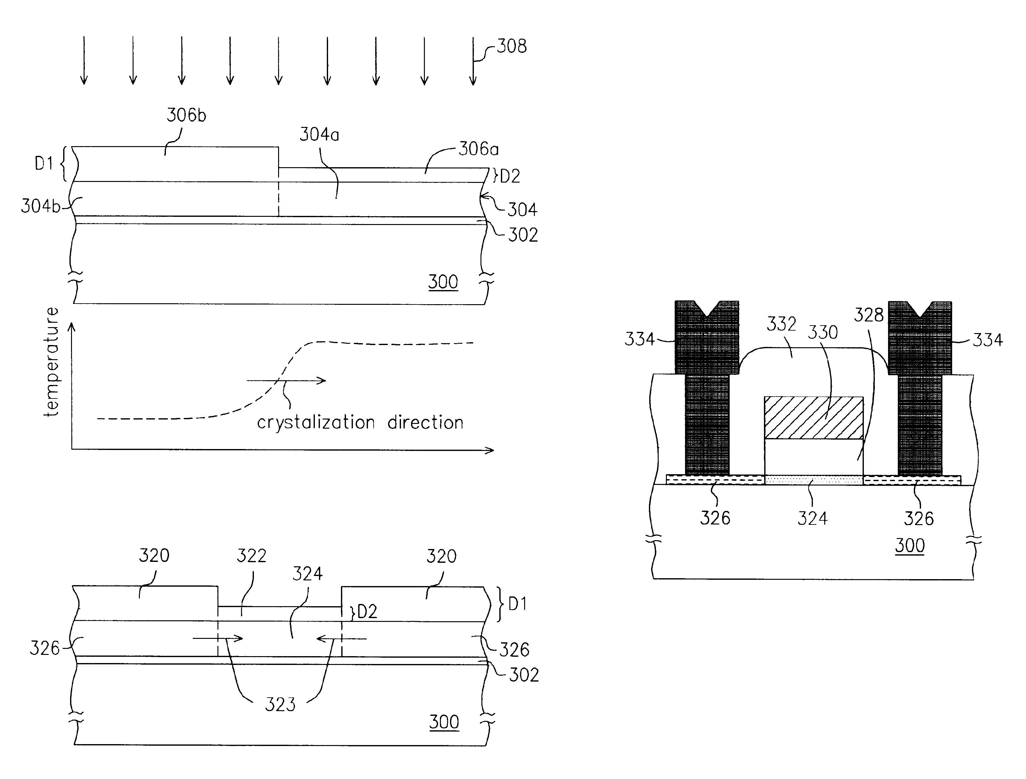
[0028]FIGS. 3A-3E are cross-sectional views illustrating a method of forming a polysilicon film according to a preferred embodiment of the present invention.

[0029]Referring to FIG. 3A, a substrate 300 is provided. The substrate 300 is comprised of, for example, a silicon wafer, a glass substrate or a plastic substrate. An insulation layer 302 is formed on the substrate 300. Preferably, the material of the insulation layer 302 is comprised of, for example, silicon dioxide, and can be formed by performing, for example, a low pressure chemical vapor deposition (LPCVD) process, a plasma enhanced chemical vapor deposition (PECVD) process or a sputtering process. The insulation layer has a thickness of, for example, about 500˜4000 Å. An amorphous silicon layer 304 is then formed on the insulation layer 302, and the amorphous silicon layer 304 can be formed by performing, for example, a LPCVD, a PECVD or a sputtering process. The amorphous silicon layer 304 has a thickness of, for example,...


PUM

PropertyMeasurementUnit
temperatureaaaaaaaaaa
thickness D1aaaaaaaaaa

Abstract

A method of fabricating polysilicon film is described. An amorphous silicon layer is formed on the substrate, an optical layer is formed on the amorphous silicon layer, wherein the optical has a first region having a first thickness and a second region having a second thickness, and the reflectivity of the first region for an excimer laser is higher than that of the second region. A laser annealing process is then preformed to transform the amorphous silicon layer into a polysilicon film.

Description

CROSS REFERENCE TO RELATED APPLICATIONS[0001]This application claims the priority benefit of Taiwan application serial no. 92120192, filed on Jul. 24, 2003.BACKGROUND OF INVENTION[0002]1. Field of the Invention[0003]The present invention relates to a method of forming a polysilicon film, and more particularly, to a method of forming a polysilicon film of thin film transistors of thin film transistor liquid crystal display (TFT-LCD).[0004]2. Description of the Related Art[0005]Generally, an active matrix liquid crystal display may be classified based on material used for fabricating thin film transistors, namely a polysilicon thin film transistor display and an amorphous silicon thin film transistor display. Because the polysilicon thin film transistor can integrate driving circuits, it can provide a higher yield and fabrication cost thereof is lower than the amorphous silicon thin film transistor. In addition, a polysilicon film can provide better electrical characteristics than an ...

Claims


Application Information

Patent Timeline
Patent Type & Authority Patents(United States)
IPC IPC(8): H01L21/00H01L21/70H01L21/84H01L21/336H01L29/786
CPCH01L29/66757H01L29/78675H01L27/1281
Inventor CHANG, MAO-YI
Owner AU OPTRONICS CORP
Why Eureka
Try Eureka