Efficient protection structure for reverse pin-to-pin electrostatic discharge

a protection structure and reverse pin technology, applied in the field of semiconductor integrated circuits, can solve the problems of esd damage, modern high-density integrated circuits are known to be vulnerable to damage,

Inactive Publication Date: 2005-07-19
TEXAS INSTR INC
View PDF15 Cites 33 Cited by
  • Summary
  • Abstract
  • Description
  • Claims
  • Application Information

AI Technical Summary

Benefits of technology

[0020]It is therefore an object of this invention to provide an electrostatic discharge (ESD) protection structure that provide forward and reverse polarity protection between device signal terminals.
[0022]It is a further object of this invention to provide such a structure in which parasitic resistance is reduced.
[0024]It is a further object of this invention to provide such a structure that reduces the parasitic resistance in the connections from the signal terminals of the device to the reverse polarity portion of the structure.
[0026]The present invention may be implemented by forming an electrostatic discharge protection structure, connected between two signal terminals of an integrated circuit. The structure includes both a transistor and a reverse-polarity protection diode within a common well. In the example of a bipolar protection transistor, the common well has the same conductivity type as that of the collector of the bipolar transistor. The first signal terminal is connected to the collector of the bipolar transistor, while the second signal terminal is connected to the emitter of the bipolar transistor and is resistively connected to the base of that transistor. The first and second signal terminals are connected to the cathode and anode of the diode. The bipolar transistor conducts ESD energy of a first polarity and the diode conducts ESD energy of the reverse polarity. The diode is constructed to have a reverse breakdown voltage greater than the triggering voltage of the bipolar transistor, so that the diode does not affect normal operation of the integrated circuit, and is not damaged by ESD stress of the first polarity.

Problems solved by technology

Modern high-density integrated circuits are known to be vulnerable to damage from the electrostatic discharge (ESD) of a charged body (human or otherwise) as it physically contacts an integrated circuit.
ESD damage occurs when the amount of charge exceeds the capability of the conduction path through the integrated circuit.
The typical ESD failure mechanisms include thermal runaway resulting in junction shorting, and dielectric breakdown resulting in gate-junction shorting (e.g., in the metal-oxide-semiconductor, or MOS, context).
While the arrangement of FIG. 2 provides excellent ESD protection for all combinations of ESD events, conventional implementations of the pin-to-pin protection, particularly in providing the additional isolated diode 15C as shown in FIG. 2, have been inefficient in practice. FIG. 3 illustrates the conventional physical implementation of the pin-to-pin ESD protection circuit illustrated in FIG. 2, in a cross-sectional view.

Method used


Image

  • Efficient protection structure for reverse pin-to-pin electrostatic discharge
  • Efficient protection structure for reverse pin-to-pin electrostatic discharge
  • Efficient protection structure for reverse pin-to-pin electrostatic discharge

Examples


Embodiment Construction

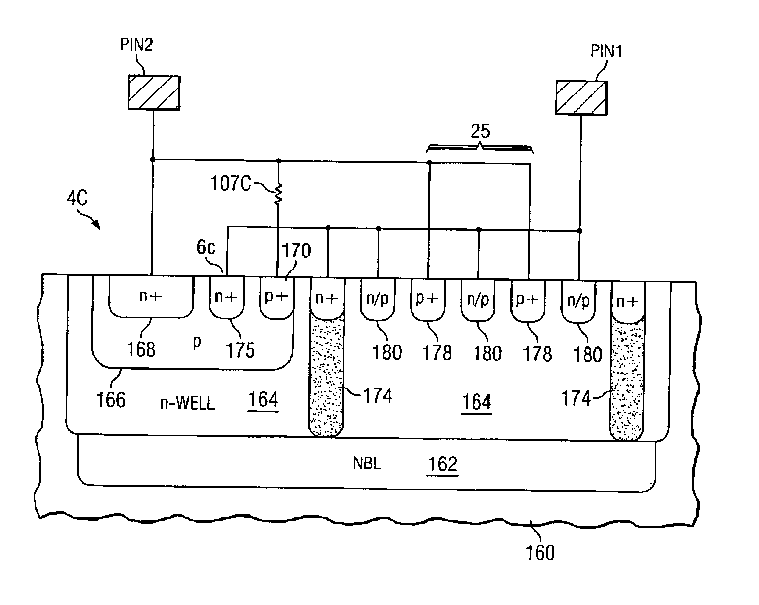
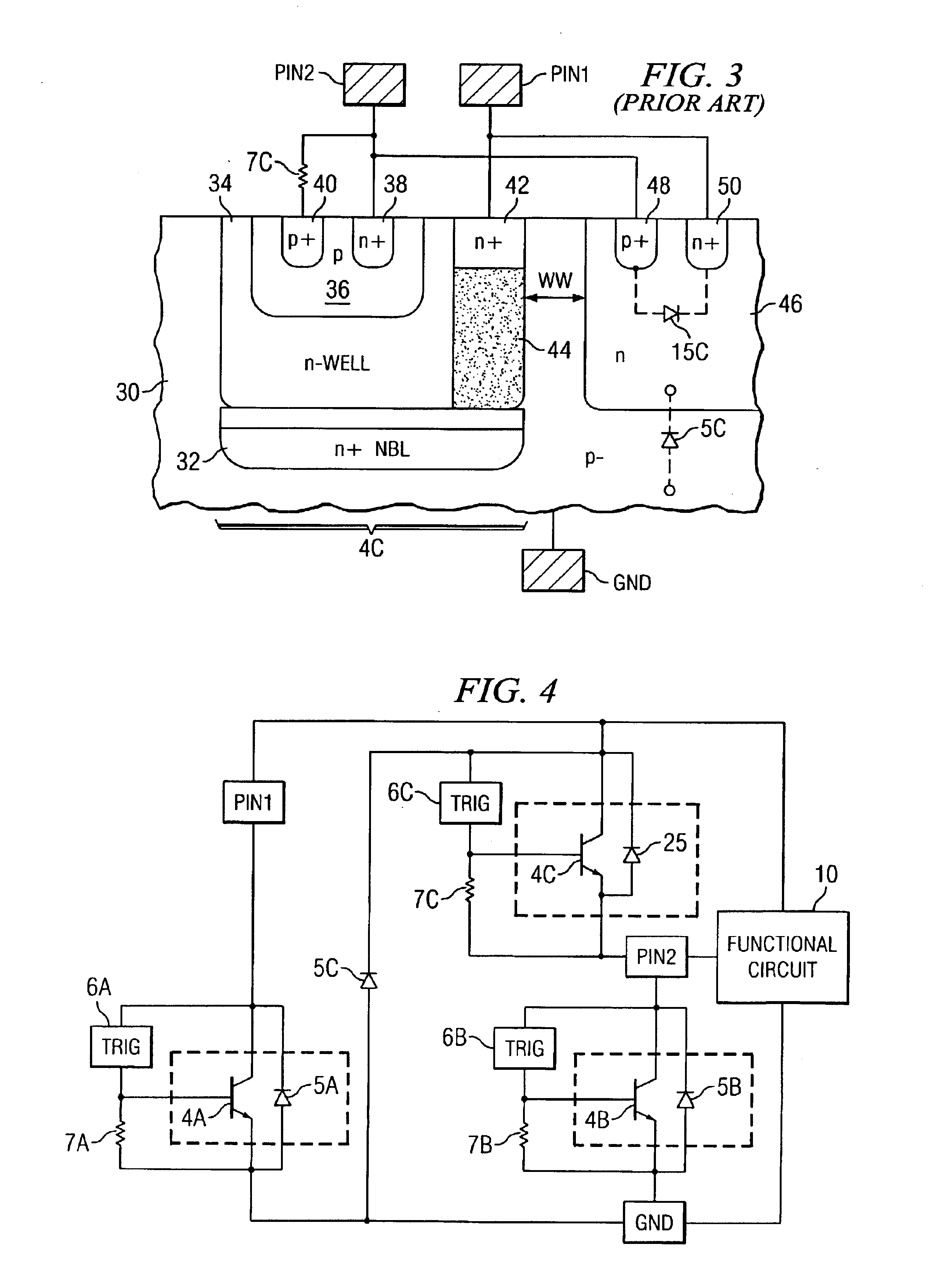
[0033]The present invention will be described in connection with its preferred embodiments, and specifically in connection with an example of this preferred embodiment of the invention involving an integrated circuit constructed according to a conventional bipolar and complementary metal-oxide-semiconductor (BiCMOS) technology. It is to be understood that this description is provided by way of example only, and is not to unduly limit the true scope of this invention as claimed.

[0034]FIG. 4 illustrates, by way of an electrical schematic, an example of an integrated circuit incorporating an ESD protection circuit according to the preferred embodiment of the invention. It is contemplated that the integrated circuit of FIG. 4 is a single-“chip” integrated circuit, in which the elements shown in FIG. 4 are all realized on the same integrated circuit device. This integrated circuit thus has a plurality of terminals for making connection to circuitry external to the integrated circuit; it ...


PUM


Abstract

An electrostatic discharge (ESD) protection structure for protecting against ESD events between signal terminals is disclosed. ESD protection is provided in a first polarity, by a bipolar transistor (4C) formed in an n-well (64; 164), having a collector contact (72; 172) to one signal terminal (PIN1) and its emitter region (68; 168) and base (66; 166) connected to a second signal terminal (PIN2). For reverse polarity ESD protection, a diode (25) is formed in the same n-well (64; 164) by a p+ region (78; 178) connected to the second signal terminal (PIN2), serving as the anode. The cathode can correspond to the n-well (64; 164) itself, as contacted by the collector contact (72; 172). By using the same n-well (64; 164) for both devices, the integrated circuit chip area required to implement this pin-to-pin protection is much reduced.

Description

CROSS-REFERENCE TO RELATED APPLICATIONS[0001]Not applicable.STATEMENT REGARDING FEDERALLY SPONSORED RESEARCH OR DEVELOPMENT[0002]Not applicable.BACKGROUND OF THE INVENTION[0003]This invention is in the field of semiconductor integrated circuits, and is more specifically directed to integrated structures for protecting such circuits from electrostatic discharge events.[0004]Modern high-density integrated circuits are known to be vulnerable to damage from the electrostatic discharge (ESD) of a charged body (human or otherwise) as it physically contacts an integrated circuit. ESD damage occurs when the amount of charge exceeds the capability of the conduction path through the integrated circuit. The typical ESD failure mechanisms include thermal runaway resulting in junction shorting, and dielectric breakdown resulting in gate-junction shorting (e.g., in the metal-oxide-semiconductor, or MOS, context).[0005]To avoid damage from ESD, modern integrated circuits incorporate ESD protection...

Claims


Application Information

Patent Timeline
Patent Type & Authority Patents(United States)
IPC IPC(8): H01L27/02H01L27/04H01L21/822H01L21/8238H01L27/06H01L27/092H03K19/003
CPCH01L27/0248H01L2924/0002H01L2924/00
Inventor BRODSKY, JONATHANSTEINHOFF, ROBERTPENDHARKAR, SAMEER P.
Owner TEXAS INSTR INC
Why Eureka
Try Eureka