Semiconductor device

A technology of semiconductor and conductor components, which is applied in the direction of semiconductor devices, semiconductor/solid-state device manufacturing, semiconductor/solid-state device components, etc., and can solve problems such as reduced heat dissipation

Inactive Publication Date: 2005-08-03
RENESAS ELECTRONICS CORP
View PDF2 Cites 33 Cited by
  • Summary
  • Abstract
  • Description
  • Claims
  • Application Information

AI Technical Summary

Problems solved by technology

[0012] However, in the MCM, the mounting area is reduced by making a plurality of semiconductor

Method used


Image

  • Semiconductor device
  • Semiconductor device
  • Semiconductor device

Examples


Embodiment 1

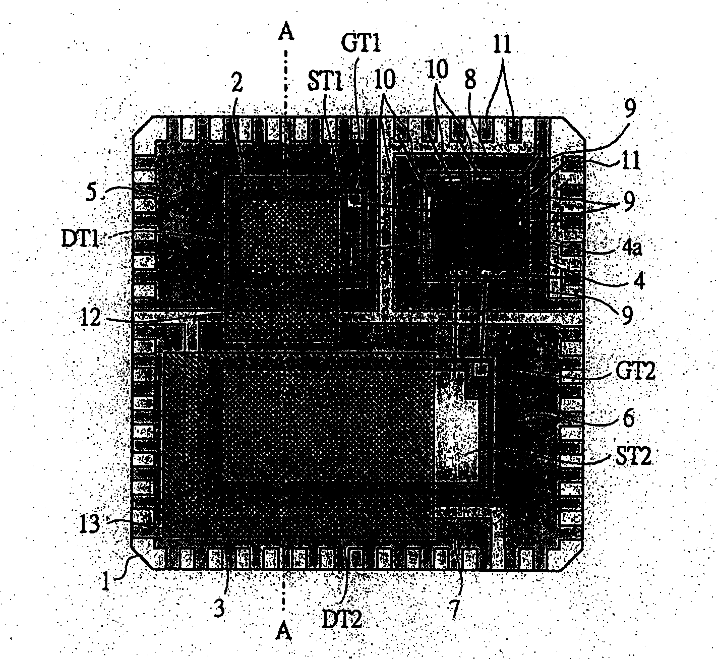
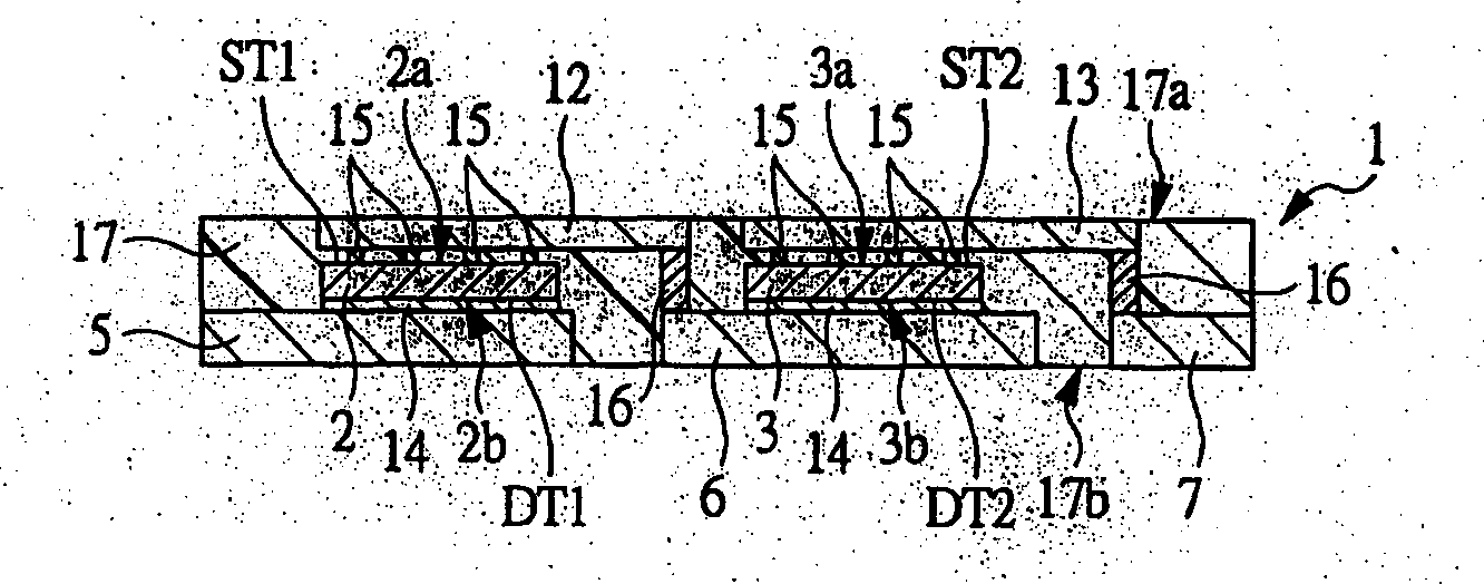
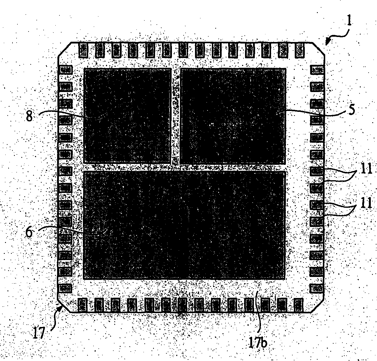
[0052] figure 1 It is a plan view showing an example of the structure of the semiconductor device (multi-chip module for non-isolated DC / DC converter) of Embodiment 1 of the present invention through a package, Figure 17 is through figure 1 The oblique view showing the interior of the semiconductor device shown in, figure 2 is shown along figure 1 A cross-sectional view of the structure of the cross-section cut by the line A-A shown in, image 3 is showing figure 1 The back view of the structure of the semiconductor device shown in, Figure 4 is showing figure 1 The external oblique view of the structure of the semiconductor device shown in, Figure 5 ~ Figure 7 are cross-sectional views each showing the structure of a semiconductor device according to a modified example of Embodiment 1 of the present invention, Figure 8 is showing figure 1 A circuit diagram of an example of an equivalent circuit when mounted in a semiconductor device (non-isolated DC / DC converter) ...

Embodiment 2

[0081] Figure 9 It is a plan view showing an example of the structure of the semiconductor device (multi-chip module for non-isolated DC / DC converter) of Embodiment 2 of the present invention through a package, Figure 10 is shown along Figure 9 A cross-sectional view of the structure of the cross-section cut along the line B-B shown in, Figure 11 is showing Figure 9 The back view of the structure of the semiconductor device shown in, Figure 12 is showing Figure 9 The external oblique view of the structure of the semiconductor device shown in .

[0082] The semiconductor device of present embodiment 2 is the same as embodiment 1, is the MCM (multi-chip module) 1 that the non-isolated type DC / DC converter is used, is to enclose the power MOSFET chip 2 for control, the power MOSFET chip 3 for synchronization and make it lead On / off driver IC chip 4 semiconductor package.

[0083] If explain the structure of the MCM1 of present embodiment 2, then as Figure 9 , Fig...

Embodiment 3

[0097] Figure 13 It is a cross-sectional view showing an example of the structure of the semiconductor device (multi-chip module for non-isolated DC / DC converter) of Embodiment 3 of the present invention, Figure 14 It is a cross-sectional view showing the structure of a semiconductor device according to a modified example of Embodiment 3 of the present invention.

[0098] The semiconductor device of the third embodiment is an MCM (multi-chip module) 1 for a non-isolated DC / DC converter, as in the first and second embodiments, and a structure for improving heat dissipation will be described.

[0099] Figure 13 In the MCM1 shown in , the heat sink 27 as a heat dissipation member is attached to the MCM1 described in Embodiment 1. That is, since the two plate-shaped lead parts (source plate-shaped lead parts 12 and 13) exposed on the surface 17a of the package 17 of the MCM1 of Example 1 have different potentials, the heat dissipation is installed via the insulating sheet 28....


PUM


Abstract

In the semiconductor device, a control power MOSFET chip 2 is disposed on the input-side plate-like lead 5 , and the drain terminal DT 1 is formed on the rear surface of the chip 2 , and the source terminal ST 1 and gate terminal GT 1 are formed on the principal surface of the chip 2 , and the source terminal ST 1 is connected to the plate-like lead for source 12 . Furthermore, a synchronous power MOSFET chip 3 is disposed on the output-side plate-like lead 6 , and the drain terminal DT 2 is formed on the rear surface of the chip 3 and the output-side plate-like lead 6 is connected to the drain terminal DT 2 . Furthermore, source terminal ST 2 and gate terminal GT 2 are formed on the principal surface of the synchronous power MOSFET chip 3 , and the source terminal ST 2 is connected to the plate-like lead for source 13 . The plate-like leads for source 12 and 13 are exposed, and therefore, it is possible to increase the heat dissipation capability of the MCM 1.

Description

technical field [0001] The present invention relates to a semiconductor device, and particularly relates to a technique effective for a semiconductor device in which a plurality of semiconductor chips are sealed in a package. Background technique [0002] In a conventional semiconductor device, the back surface of a heat sink (first conductor member) is bonded to the surface of each semiconductor chip by soldering, and the surface of a second conductor member is bonded to the back surface of each semiconductor chip. In addition, the back surface of the third conductor member is bonded to the surface of the heat sink by soldering, and furthermore, a land of a predetermined semiconductor chip is electrically connected to a control terminal through a bonding wire. Each semiconductor chip, the heat sink, the surface of the second conductor member, the back surface of the third conductor member, bonding wires, and part of the control terminal are packaged with resin (for example,...

Claims


Application Information

Patent Timeline
IPC IPC(8): H01L23/28H01L21/52H01L23/02H01L23/34H01L23/36H01L23/495H01L25/04H01L25/07H01L25/18H01L27/00
CPCH01L24/37H01L2924/01002H01L2224/73221H01L24/29H01L2224/73219H01L24/40H01L24/45H01L24/06H01L2224/48137H01L2224/16245H01L2224/32245H01L24/41H01L2224/13144H01L23/49568H01L2224/73253H01L2924/01047H01L2924/01004H01L2924/01006H01L2924/19041H01L24/48H01L24/16H01L2224/0603H01L2924/01079H01L23/49575H01L23/49562H01L2924/14H01L2224/29339H01L2224/05553H01L24/73H01L24/13H01L2924/01005H01L2924/01082H01L2224/49111H01L2224/13099H01L2224/05599H01L2224/45144H01L2924/13091H01L24/34H01L2924/30107H01L2924/014H01L24/49H01L2224/48247H01L2924/19043H01L2224/48599H01L24/32H01L2924/01033H01L2224/85399H01L2924/00014H01L2924/01075H01L2224/40137H01L2224/40249H01L2924/1306H01L2224/0401H01L2224/29294H01L2924/181H01L2224/40245H01L2224/371H01L2224/84801H01L2224/83801H01L2224/8385H01L2224/8485H01L24/84H01L2924/00H01L2924/00012F16L55/00
Inventor 川岛彻也三岛彰
Owner RENESAS ELECTRONICS CORP
Why Eureka
Try Eureka