Structures for improving heat dissipation in stacked semiconductor packages

a technology of semiconductor packaging and structure, applied in the direction of semiconductor devices, semiconductor/solid-state device details, electrical devices, etc., can solve the problems of degrading the performance of the bottom die, difficult to effectively dissipate the heat generated by the top and bottom dies,

Inactive Publication Date: 2005-07-19
AMKOR TECH SINGAPORE HLDG PTE LTD
View PDF99 Cites 155 Cited by
  • Summary
  • Abstract
  • Description
  • Claims
  • Application Information

AI Technical Summary

Problems solved by technology

One disadvantage of stacked semiconductor packages is that it is difficult to effectively dissipate the heat generated by t

Method used


Image

  • Structures for improving heat dissipation in stacked semiconductor packages
  • Structures for improving heat dissipation in stacked semiconductor packages
  • Structures for improving heat dissipation in stacked semiconductor packages

Examples


Embodiment Construction

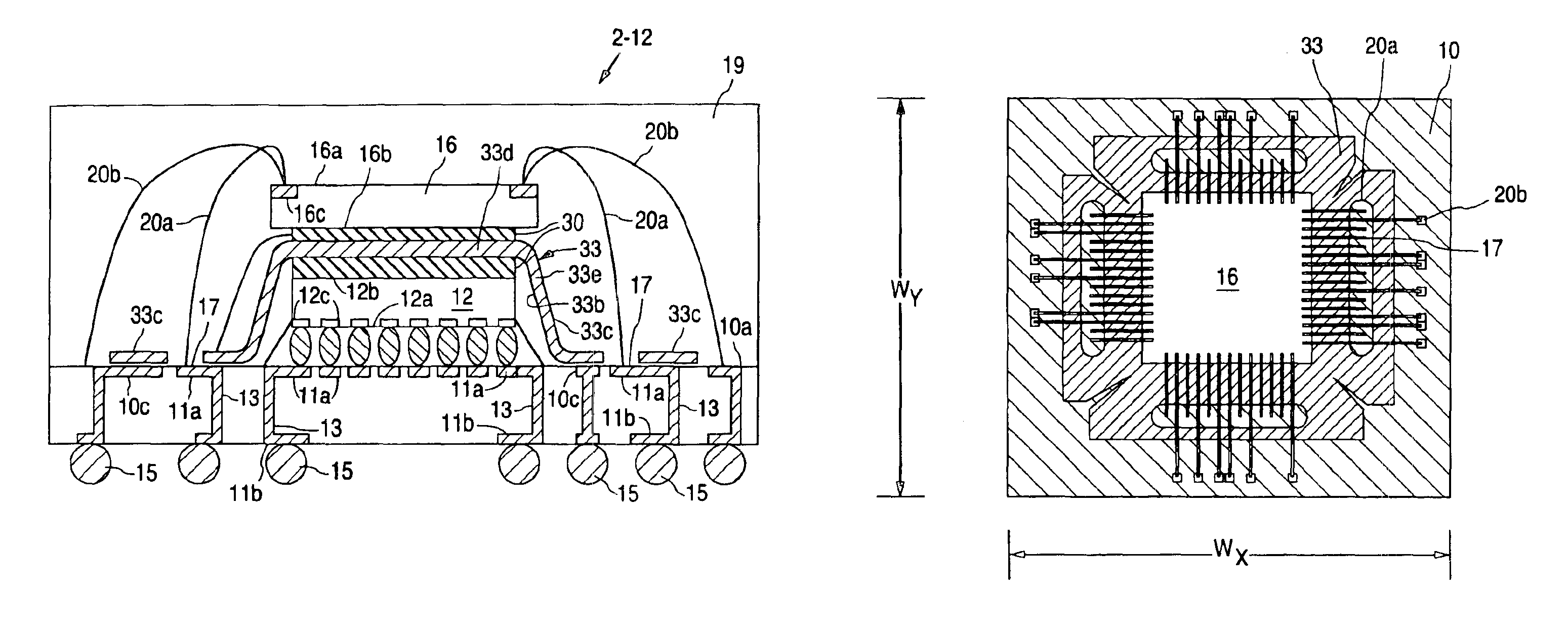
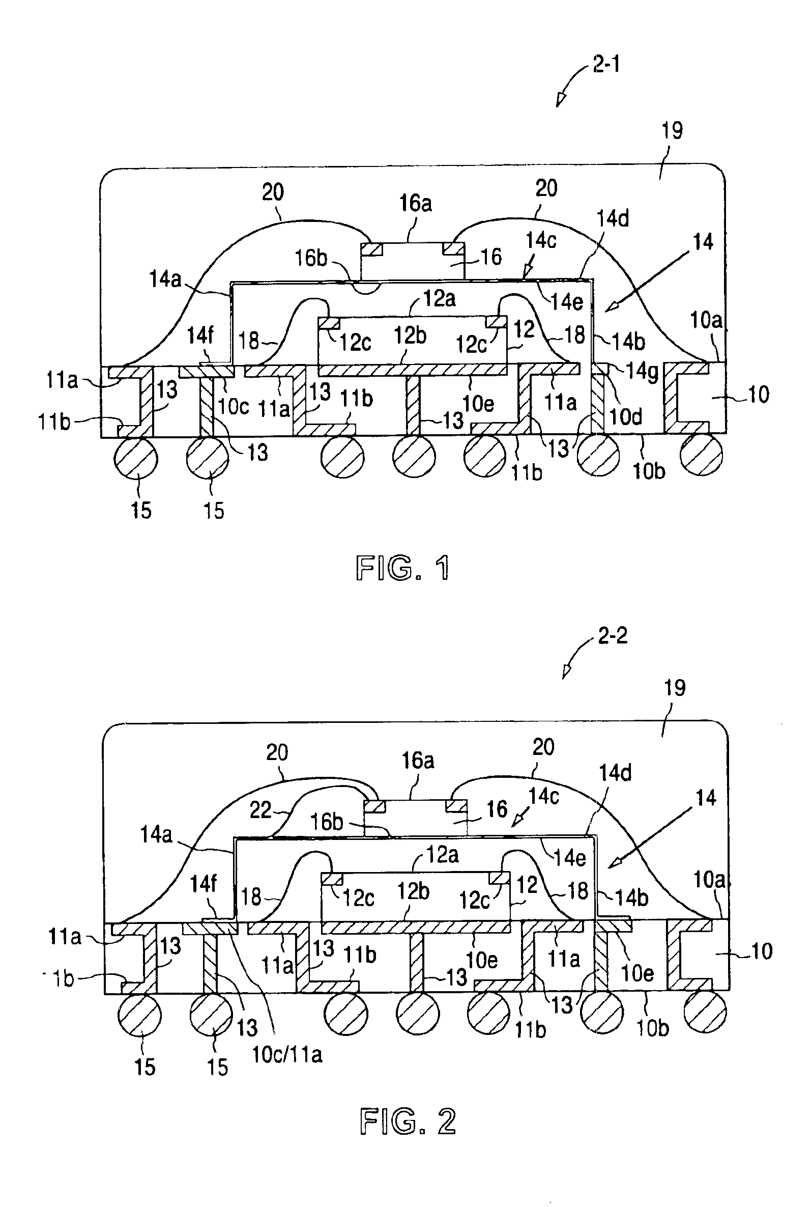
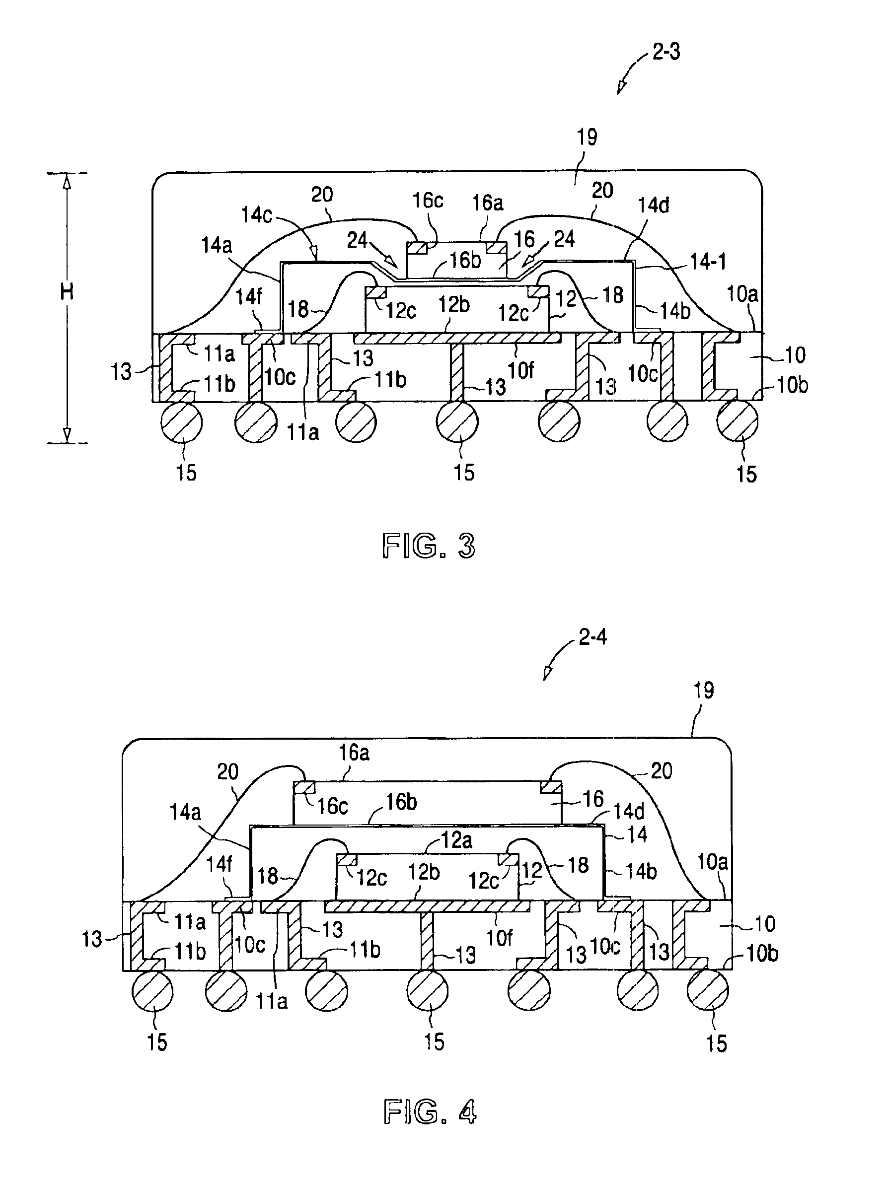
[0032]FIG. 1 is a cross-sectional view of a semiconductor package 2-1 including a support structure 14, according to one embodiment of the present invention. Semiconductor package 2-1 includes a rectangular substrate 10 having an upward-facing first surface 10a and an opposite downward-facing second surface 10b. A rectangular first die 12 having an upward-facing active first surface 12a and an opposing downward-facing inactive second surface 12b is mounted on a metal die pad 10e of first surface 10a. Die pad 10e may be thermally coupled by a via 13 to a conductive ball 15 on second surface 10b substrate 10 to transfer heat from first die 12, and also may be electrically coupled (sometimes also stated as “electrically connected” herein) through those structures to an external reference voltage so as to provide the voltage to second surface 12b of first die 12.

[0033]A free-standing support structure 14 superimposes first die 12 and includes a vertically oriented first side 14a, an opp...


PUM


Abstract

Semiconductor packages including at least two semiconductor dies are disclosed. A first die is mounted on a substrate, which may be a metallized laminate or a leadframe. A rigid support structure is mounted on the substrate over the first die. The support structure may be thermally coupled to the substrate, and also may be electrically coupled to the substrate. A second die is mounted on the support structure, which spaces the second die away from the first die. Encapsulant fills the volume within the support structure, including the vertical space between the pair of dies. In an alternative package embodiment, a heat spreader formed of a flexible metal sheet may be thermally coupled between the two stacked dies. The heat spreader transfers heat from the first and second dies to a heat sink of the substrate. The support structure and the heat spreader mitigate the transfer of heat between the first and second dies.

Description

CROSS-REFERENCE TO RELATED APPLICATION[0001]This application is a division of U.S. patent application Ser. No. 10 / 013,396, filed on Dec. 7, 2001, now U.S. Pat. No. 6,737,750, issued on May 18, 2004, and incorporated herein by reference in its entirety.BACKGROUND[0002]1. Field of the Invention[0003]The present invention relates to a semiconductor package and a method for fabricating a semiconductor package.[0004]2. Related Art[0005]Semiconductor packages that include stacked semiconductor dies (otherwise known as semiconductor “chips” or “integrated circuits”) are becoming increasingly popular. Such packages allow dies that perform the same function (e.g., two memory dies) or different functions (e.g., a processor die and a memory die) to be combined into a single package. This improves density and is especially useful in applications where package size is important, such as in cell phones, PDAs, camcorders, and other wireless consumer products.[0006]Conventional stacked semiconducto...

Claims


Application Information

Patent Timeline
IPC IPC(8): H01L25/065H01L23/28H01L23/31
CPCH01L23/3128H01L23/552H01L25/0657H01L2224/16145H01L2224/32014H01L2224/32145H01L2224/48091H01L2224/48227H01L2224/73253H01L2225/0651H01L2225/06575H01L2225/06582H01L2225/06589H01L2924/01079H01L2924/15311H01L2924/16152H01L2924/19041H01L2924/19105H01L2924/3025H01L2924/00014H01L2224/73265H01L2224/32225H01L24/48H01L2224/45124H01L2924/00H01L2224/73204H01L2224/16225H01L2224/32245H01L2224/48247H01L2924/00012H01L2224/73215H01L2224/45144H01L2224/45147H01L24/45H01L24/73H01L2924/14H01L2924/1627H01L2224/05571H01L2224/05573H01L2924/181H01L2224/05554H01L2924/10162H01L24/49H01L2224/49171H01L24/05H01L2224/05599
Inventor HOFFMAN, PAUL ROBERTZOBA, DAVID ALBERT
Owner AMKOR TECH SINGAPORE HLDG PTE LTD
Why Eureka
Try Eureka