Methods of forming a nonvolatile memory device having a local SONOS structure that use spacers to adjust the overlap between a gate electrode and a charge trapping layer

a nonvolatile memory and local sonos technology, applied in the direction of semiconductor devices, electrical devices, transistors, etc., can solve the problems of degrading the reliability of the memory device, increasing the susceptibility to photolithographic processing misalignment,

Active Publication Date: 2005-08-09
SAMSUNG ELECTRONICS CO LTD
View PDF3 Cites 31 Cited by
  • Summary
  • Abstract
  • Description
  • Claims
  • Application Information

AI Technical Summary

Problems solved by technology

Accordingly, as the degree of integration of a device increases, the susceptibility to misalignment in photolithographic processing increases.
Irregularity in the length of “A” may result in irregular characteristics of a memory cell, which may ultimately degrade the reliability of a memory device.

Method used


Image

  • Methods of forming a nonvolatile memory device having a local SONOS structure that use spacers to adjust the overlap between a gate electrode and a charge trapping layer
  • Methods of forming a nonvolatile memory device having a local SONOS structure that use spacers to adjust the overlap between a gate electrode and a charge trapping layer
  • Methods of forming a nonvolatile memory device having a local SONOS structure that use spacers to adjust the overlap between a gate electrode and a charge trapping layer

Examples


Embodiment Construction

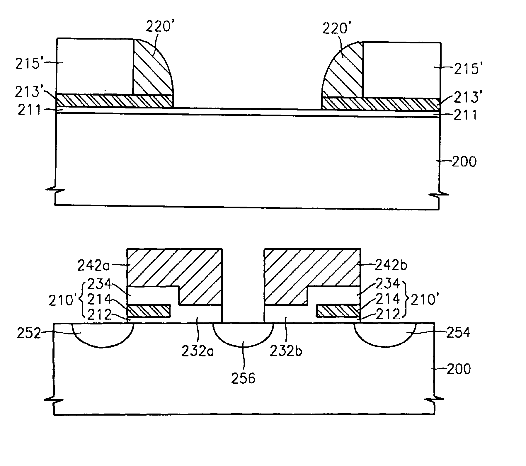
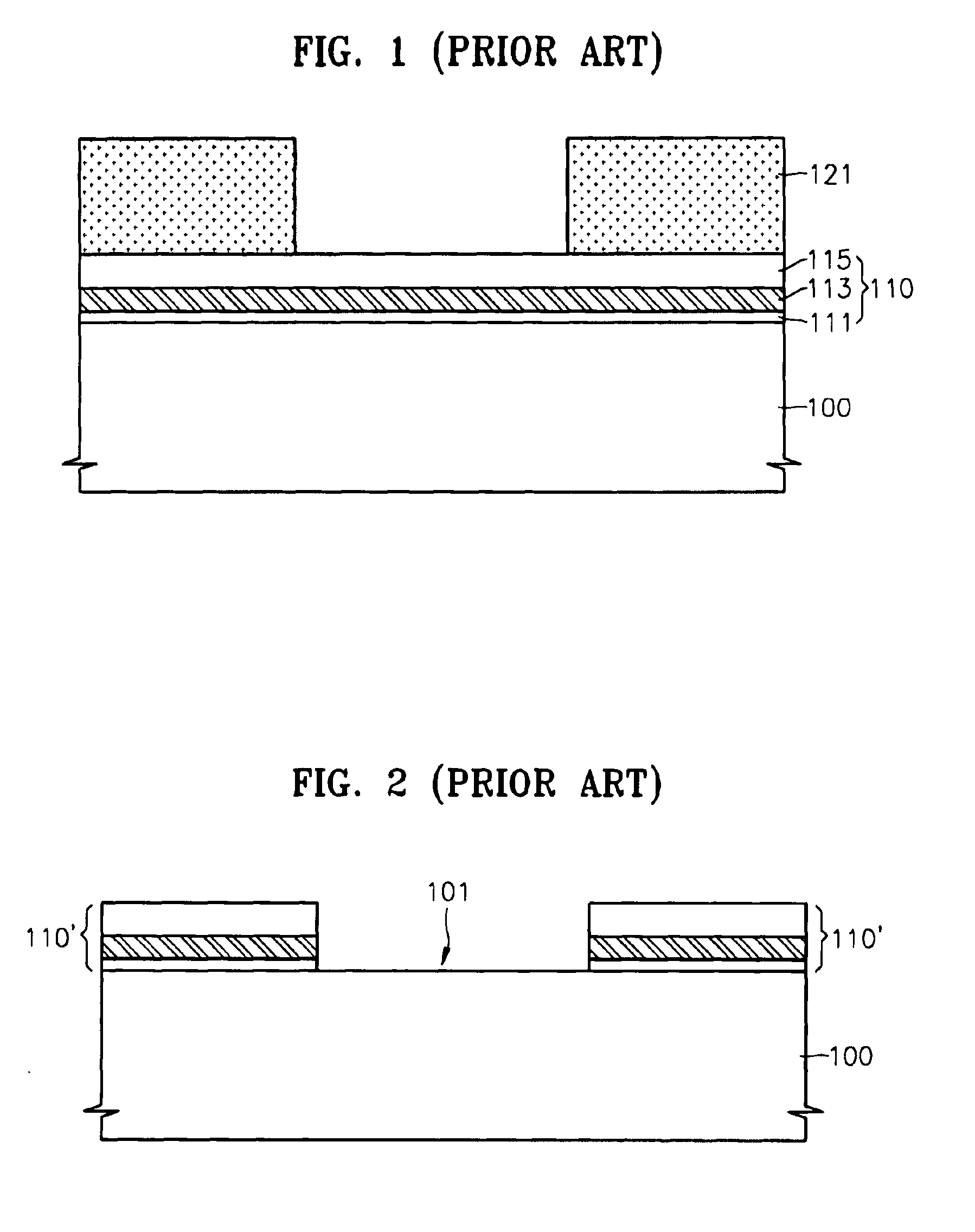
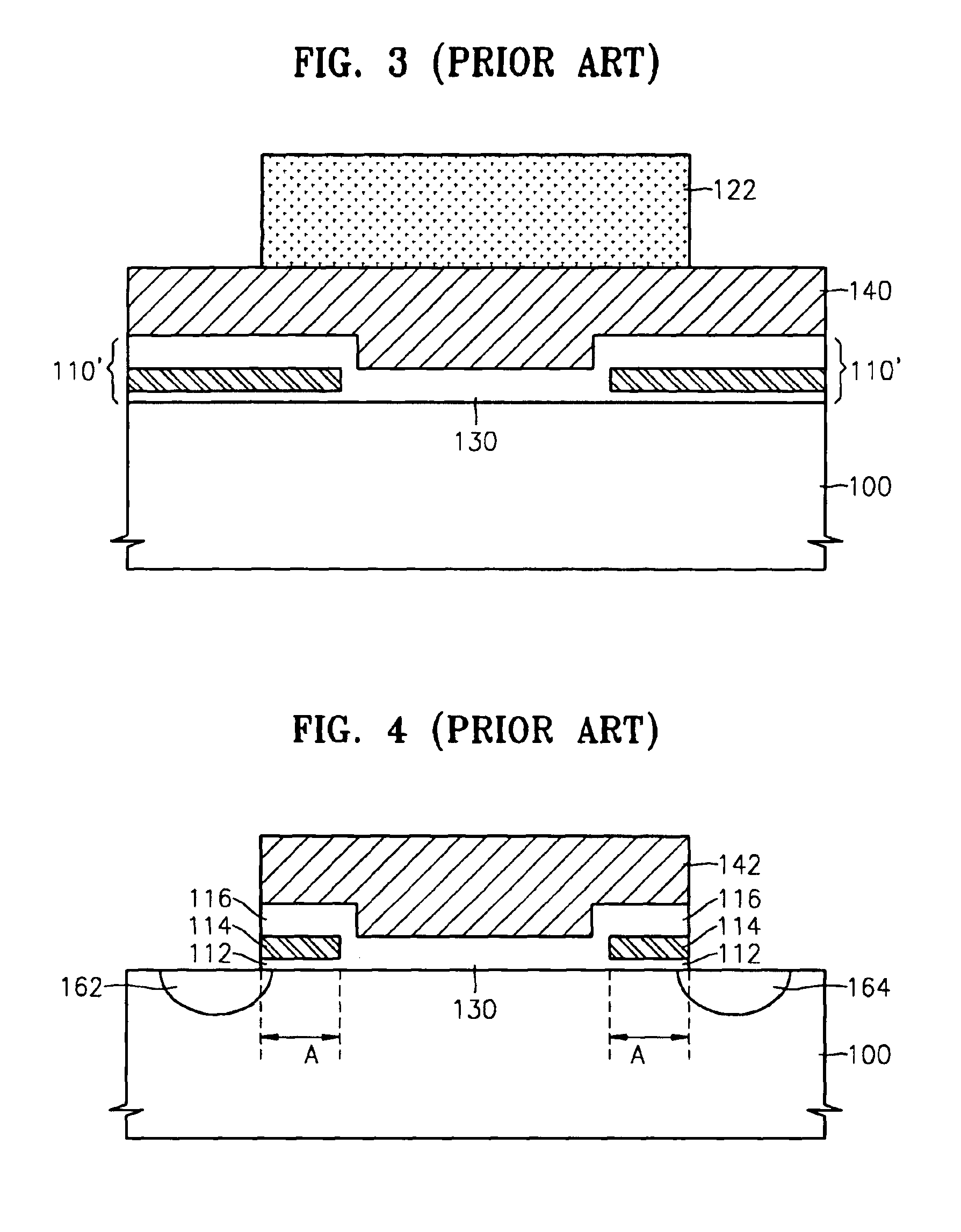
[0019]While the invention is susceptible to various modifications and alternative forms, specific embodiments thereof are shown by way of example in the drawings and will herein be described in detail. It should be understood, however, that there is no intent to limit the invention to the particular forms disclosed, but on the contrary, the invention is to cover all modifications, equivalents, and alternatives falling within the spirit and scope of the invention as defined by the claims. Like numbers refer to like elements throughout the description of the figures. In the figures, the dimensions of layers and regions are exaggerated for clarity. It will also be understood that when an element, such as a layer, region, or substrate, is referred to as being “on” another element, it can be directly on the other element or intervening elements may be present. In contrast, when an element, such as a layer, region, or substrate, is referred to as being “directly on” another element, there...


PUM


Abstract

A nonvolatile memory device is formed by forming a first oxide layer on a substrate. A nitride layer is formed on the first oxide layer. A second oxide layer is formed on the nitride layer. The second oxide layer is patterned so as to expose the nitride layer. A first polysilicon layer is formed on the second oxide layer and the exposed portion of the nitride layer. The first polysilicon layer and the nitride layer are etched so as to expose the second oxide layer and the first oxide layer and to form polysilicon spacers on the nitride layer. The polysilicon spacers are etched so as to expose portions of the nitride layer. The exposed portions of the nitride layer may function as charge trapping layers. The exposed portion of the first oxide layer is etched to expose a portion of the substrate. A third oxide layer is formed on the exposed portion of the substrate, the exposed portions of the nitride layer, and the second oxide layer. A second polysilicon layer is formed on the third oxide layer. The second polysilicon layer is planarized so as to expose the second oxide layer. The second polysilicon layer may function as a gate electrode that overlaps portions of the charge trapping layers. The third oxide layer may function as a gate-insulating layer.

Description

RELATED APPLICATION[0001]This application claims the benefit of and priority to Korean Patent Application No. 2002-48967, filed Aug. 19, 2002, the disclosure of which is hereby incorporated herein by reference.FIELD OF THE INVENTION[0002]The present invention relates to a method for fabricating nonvolatile memory devices, and more particularly, to method of fabricating nonvolatile memory devices having a local SONOS (Silicon-Oxide-Nitride-Oxide-Silicon) structure.BACKGROUND OF THE INVENTION[0003]In general, semiconductor memory devices used for storing data are divided into two types: volatile and nonvolatile. A volatile memory device loses stored data when the power supply is interrupted, while a nonvolatile memory device maintains the stored data when the power supply is interrupted. Therefore, in applications where the power supply is not always continuous, occasionally interrupted, requires the use of low power on occasion, such as in a mobile communication system, a memory card...

Claims


Application Information

Patent Timeline
Patent Type & Authority Patents(United States)
IPC IPC(8): H01L21/70H01L27/115H01L21/8246H01L21/8247H01L29/788H01L29/792
CPCH01L27/115H01L27/11568H10B69/00H10B43/30
Inventor KIM, SEONG-GYUN
Owner SAMSUNG ELECTRONICS CO LTD
Why Eureka
Try Eureka