3-transistor OTP ROM using CMOS gate oxide antifuse

a technology of gate oxide and otp rom, which is applied in the field of one-time-programmable otp roms using cmos gate oxide anti-fuses, can solve the problems of difficult to obtain uniform breakdown properties, poor anti-fuse properties, and additional processes, and achieves the effect of higher integration

Inactive Publication Date: 2005-08-09
KOREA ADVANCED INST OF SCI & TECH
View PDF3 Cites 76 Cited by
  • Summary
  • Abstract
  • Description
  • Claims
  • Application Information

AI Technical Summary

Benefits of technology

[0015]Yet another object of the present invention is to provide an OTP ROM that can be higher integrated using an array structure.

Problems solved by technology

These structures, however, had a difficulty in implementation as follows and a problem in that the properties of the antifuse are poor.
Firstly, the above schemes required additional process in the existing standard CMOS process.
Secondly, since it is difficult to uniformly control the thickness of an insulator through the process, it is also difficult to obtain uniform breakdown properties.
Accordingly, there is a problem that a variation in a programming voltage of the antifuse is high.
Lastly, an existing ONO structure uses the antifuse of a capacitor type and has a complicate control circuit.
Thus, there is a disadvantage that a large area per unit cell is needed.
Furthermore, its applicable fields are limited to the recovery of defective memory cells having only several bit capacity.
This structure, however, also has disadvantages that it requires an additional mask in the existing standard CMOS process and occupies a large area since one n-well per bit is used.

Method used


Image

  • 3-transistor OTP ROM using CMOS gate oxide antifuse
  • 3-transistor OTP ROM using CMOS gate oxide antifuse
  • 3-transistor OTP ROM using CMOS gate oxide antifuse

Examples


Embodiment Construction

[0040]The present invention will now be described in detail in connection with preferred embodiments with reference to the accompanying drawings.

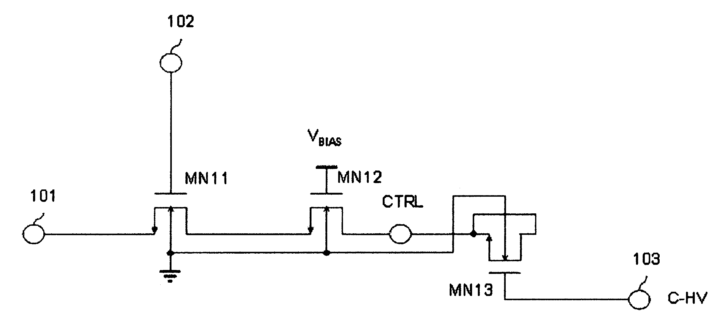
[0041]FIG. 1 is a circuit diagram showing the construction of a 3-transistor OTP ROM cell according to an embodiment of the present invention.

[0042]Referring to FIG. 1, the OTP ROM cell according to an embodiment of the present invention includes three input terminals 101 to 103 and three nMOSFET devices MN11 to MN13.

[0043]The interconnection relationship among the components will now be described.

[0044]The first NMOS transistor MN11 has a gate for forming the second input terminal 102, and a drain connected to a source of the second NMOS transistor MN12. Also, the source of the first NMOS transistor MN11 forms the first input terminal 101. The second NMOS transistor MN12 has a gate to which a bias voltage VBIAS is applied and a drain connected to a control terminal CTRL of the third NMOS transistor MN13. A gate of the third NMOS transistor...


PUM


Abstract

The present invention relates to an OTP ROM using a CMOS gate oxide antifuse. According to an embodiment of the present invention, in an OTP ROM cell having a first input terminal, a second input terminal and a third input terminal, wherein the OTP ROM stores data by means of a voltage applied to the first to third input terminals, the OTP ROM cell includes a cell access transistor having a gate and drain forming the second input terminal and a source forming the first input terminal, wherein the cell access transistor is activated by a voltage applied to between the gate and source, a high-voltage blocking transistor having a gate, a drain and a source connected to the drain of the cell access transistor, wherein the high-voltage blocking transistor allows the current to flow from the drain to the source by means of a bias voltage applied to the gate, thus blocking the high voltage applied to the third input terminal from being directly applied to the cell access transistor, and an antifuse transistor having a gate forming the third input terminal, and source and drain both of which are connected to each other and are then connected to the drain of the high-voltage blocking transistor, wherein a high voltage is applied to the third input terminal and if the cell access transistor is activated, gate oxide is broken and shorted.

Description

BACKGROUND OF THE INVENTION[0001]1. Field of the Invention[0002]The present invention relates to a semiconductor memory device, and more particularly, to an OTP (One-Time Programmable) ROM using a CMOS gate oxide antifuse.[0003]2. Background of the Related Art[0004]In fabricating a CMOS OTP nonvolatile memory, an antifuse device has been widely used. The antifuse is the opposite of a regular fuse. The antifuse is electrically an “open circuit” in a normal state, but becomes a “short circuit” if an insulator is broken through application of a high voltage, if necessary. An OTP ROM can be implemented with these two states.[0005]A device used as an antifuse is mainly a metal-oxide-metal. Recently, there has been proposed a structure in which an Oxide-Nitride-Oxide (ONO) capacitor used in DRAM process is used as the antifuse. These structures, however, had a difficulty in implementation as follows and a problem in that the properties of the antifuse are poor.[0006]Firstly, the above sch...

Claims


Application Information

Patent Timeline
Patent Type & Authority Patents(United States)
IPC IPC(8): G11C11/34G11C17/00G11C17/16
CPCG11C17/16G11C17/00
Inventor LEE, KWYROKIM, JINBONGCHA, HYOUK-KYU
Owner KOREA ADVANCED INST OF SCI & TECH
Why Eureka
Try Eureka