Mechanism for inter-fab mask process management

a process management and semiconductor technology, applied in the field of semiconductor mask process management, can solve the problems of increasing the complexity of processing and manufacturing ics, etc., and reducing the number of interconnected devices per ic area. , the effect of increasing the complexity of manufacturing ics

Inactive Publication Date: 2005-08-09
TAIWAN SEMICON MFG CO LTD
View PDF7 Cites 13 Cited by
  • Summary
  • Abstract
  • Description
  • Claims
  • Application Information

AI Technical Summary

Problems solved by technology

However, these advances have increased the complexity of processing and manufacturing ICs and, for these advances to be realized, similar developments in IC processing and manufacturing have been needed.
As the geometry of such devices is reduced to the submicron or deep submicron level, the IC's active device density (i.e., the number of devices per IC area) and functional density (i.e., the number of interconnected devices per IC area) has become limited by the fabrication process.
This further increases the complexity of producing ICs, as companies and their customers may be separated not only geographically, but also by time zones, making effective communication more difficult.
Furthermore, the cost of fabrication of lithographic masks or reticles increases as device design rules scale down and the management of such masks becomes an ever increasing concern.
The valuable masks and / or reticles can be shared between fabrication facilities, however the management of reticles and / or masks can provide problems in organization such as communication problems between fabs, wherein different definitions or manufacturing executing systems (MES) may be employed.

Method used


Image

  • Mechanism for inter-fab mask process management
  • Mechanism for inter-fab mask process management
  • Mechanism for inter-fab mask process management

Examples


Embodiment Construction

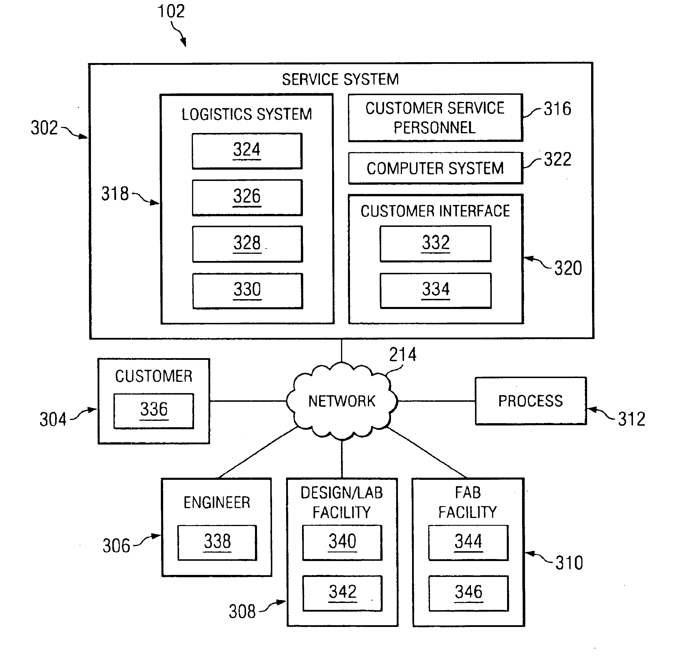
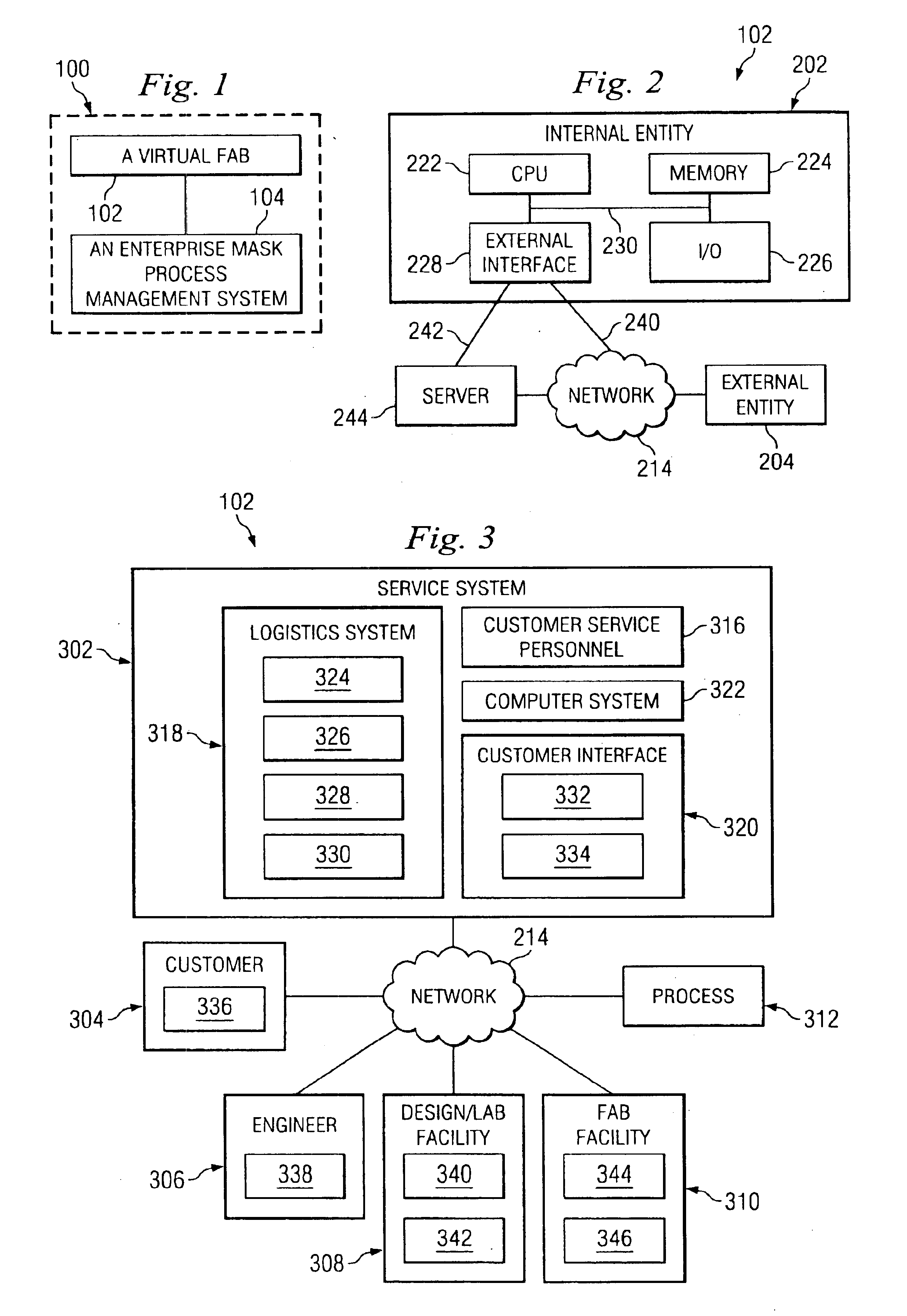
[0017]The present disclosure relates generally to the field of semiconductor manufacturing and, more particularly, to a system and method for providing an effective mask process management system in a semiconductor manufacturing environment. It is understood, however, that the following disclosure provides many different embodiments, or examples, for implementing different features of the disclosure. Specific examples of components and arrangements are described below to simplify the present disclosure. These are, of course, merely examples and are not intended to be limiting. In addition, the present disclosure may repeat reference numerals and / or letters in the various examples. This repetition is for the purpose of simplicity and clarity and does not in itself dictate a relationship between the various embodiments and / or configurations discussed.

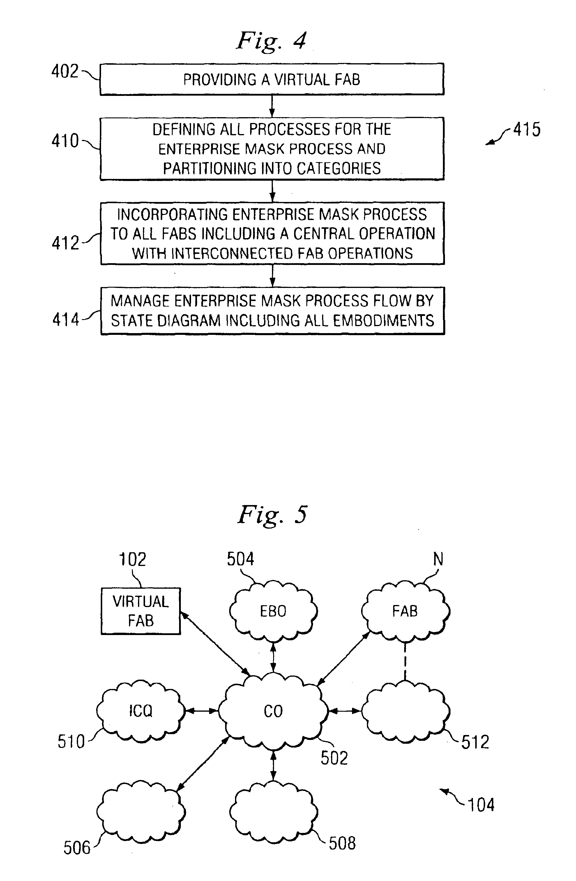
[0018]Referring to FIG. 1, in one embodiment, a system 100 for providing an effective mask process management system in a semiconductor ...


PUM


Abstract

A software mechanism is provided for inter-fab mask process management. The mechanism is used for tracking and managing a plurality of lithographic masks through a semiconductor manufacturing environment. A virtual fab is established with a plurality of entities, each entity associated with an internal process to a semiconductor fab or an external process to the semiconductor fab. A state diagram tracks the plurality of lithographic masks through the plurality of entities of the virtual fab. Each of the plurality of lithographic masks is placed at a pre-determined state of the state diagram and a future location for each of the masks in the virtual fab is determined via the state diagram.

Description

BACKGROUND[0001]The present disclosure relates generally to the field of semiconductor manufacturing and, more particularly, to a system and method for semiconductor mask process management.[0002]The semiconductor integrated circuit (IC) industry has experienced rapid growth. Technological advances in IC materials and design have produced generations of ICs where each generation has smaller and more complex circuits than the previous generation. However, these advances have increased the complexity of processing and manufacturing ICs and, for these advances to be realized, similar developments in IC processing and manufacturing have been needed. For example, an IC is formed by creating one or more devices (e.g., circuit components) on a substrate using a fabrication process. As the geometry of such devices is reduced to the submicron or deep submicron level, the IC's active device density (i.e., the number of devices per IC area) and functional density (i.e., the number of interconn...

Claims


Application Information

Patent Timeline
Patent Type & Authority Patents(United States)
IPC IPC(8): H01L21/00
CPCH01L21/67276
Inventor KUO, BIRGIE
Owner TAIWAN SEMICON MFG CO LTD
Why Eureka
Try Eureka