Method for fabricating surface acoustic wave filter package
- Summary
- Abstract
- Description
- Claims
- Application Information
AI Technical Summary
Benefits of technology
Problems solved by technology
Method used
Image
Examples
Embodiment Construction
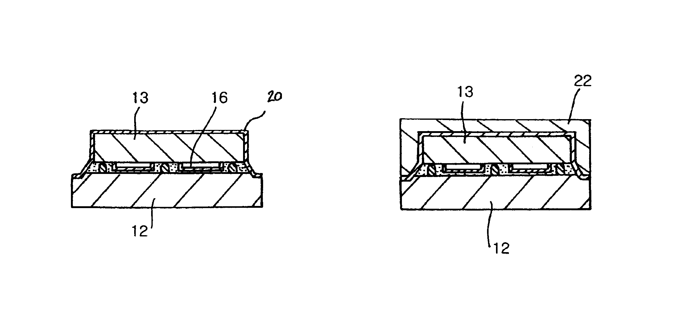
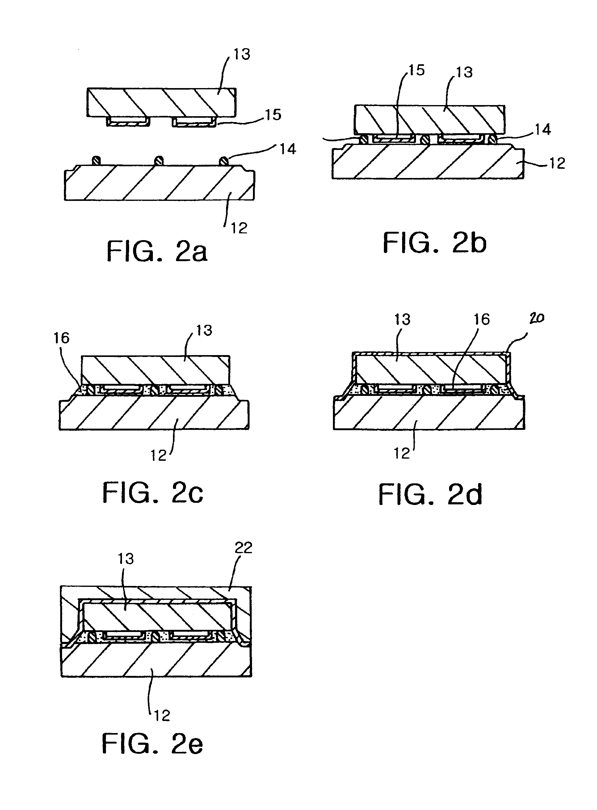
[0022]The present invention provides a method for fabricating a surface acoustic wave filter chip package comprising the steps of mounting the surface acoustic wave filter chip on a substrate; forming a underfill in a space between the substrate and the surface acoustic wave filter chip; forming a metal shield layer on a whole outer wall of the surface acoustic wave filter chip by spraying; and molding resins on the metal shield layer.
[0023]According to an embodiment of the present invention, the SAW filter chip is provided with plural protector structures in order to form an air gap on a lower side surface of the SAW filter chip, and mounted on the substrate by flip chip bonding.
[0024]According to a preferred embodiment of the present invention, a structurally simplified appearance of the SAW filter package, for example a rectangular parallelepiped, can be obtained by molding the SAW filter chip package with EMC (epoxy molding compound) so as to wholly cover the metal shield layer....
PUM
| Property | Measurement | Unit |
|---|---|---|
| Electrical conductor | aaaaa | aaaaa |
Abstract
Description
Claims
Application Information
 - R&D
- Intellectual Property
- Life Sciences
- Materials
- Tech Scout
- Unparalleled Data Quality
- Higher Quality Content
- 60% Fewer Hallucinations
Browse by: Latest US Patents, China's latest patents, Technical Efficacy Thesaurus, Application Domain, Technology Topic, Popular Technical Reports.
© 2025 PatSnap. All rights reserved.Legal|Privacy policy|Modern Slavery Act Transparency Statement|Sitemap|About US| Contact US: help@patsnap.com


