Stacked semiconductor die assembly having at least one support

a technology of semiconductor dies and supports, applied in semiconductor devices, semiconductor/solid-state device details, electrical devices, etc., can solve problems such as significant overlap and exceed conventional tolerances, and achieve the effects of exceeding conventional tolerances, saving time and cost, and increasing stack siz

Active Publication Date: 2005-08-16
AMKOR TECH SINGAPORE HLDG PTE LTD
View PDF25 Cites 173 Cited by
  • Summary
  • Abstract
  • Description
  • Claims
  • Application Information

AI Technical Summary

Benefits of technology

[0008]The present invention includes structures and methods that allow a plurality of semiconductor dies to be stacked in a compact manner in semiconductor packages and in other electronic assemblies.
[0010]Practitioners will appreciate that, with the above-described embodiment, the second semiconductor die may be stacked on the active surface of the first semiconductor die and overlap the one or more of the peripheral sides of the first semiconductor die, provided that the bond pads of the first semiconductor die are not obstructed. The overlap may be significant and may exceed conventional tolerances because of the provision of the at least one support beneath the second semiconductor die. In addition, since there is no overlap of the first semiconductor die's bond pads by the second semiconductor die, the wirebonding step for each of these two stacked semiconductor die may be performed together in a single wirebonding operation, thereby saving time and cost in the assembly process.
[0011]A further embodiment increases the size of the stack by attaching at least one second-level support on the active surface of the first semiconductor die adjacent to the second semiconductor die, using an electrically insulative adhesive layer having the same thickness as the adhesive layer coupling the second semiconductor die to the first semiconductor die. The second-level support(s) has the same thickness (i.e., vertical height) as the second semiconductor die. Accordingly, the active surface of the second semiconductor die and the upper surface of the at least one second-level support are coplanar. A third semiconductor die having an uniformly-thick, electrically insulative, adhesive layer over its entire inactive surface is then attached to the coplanar active surface of the second semiconductor die and the upper surface of the at least one second-level support. The third semiconductor die is sized and disposed so that the third semiconductor die does not overlap the bond pads of the underlying second semiconductor die, notwithstanding that the third die may overhang one or more edges of the active surface of the second semiconductor die and may overlap the bond wires of the first semiconductor die, provided that there is no adverse contact with the bond wires of the first semiconductor die. The process can be repeated to provide stacks of four, five, six, or more levels of semiconductor dies and support(s).

Problems solved by technology

The overlap may be significant and may exceed conventional tolerances because of the provision of the at least one support beneath the second semiconductor die.

Method used


Image

  • Stacked semiconductor die assembly having at least one support
  • Stacked semiconductor die assembly having at least one support
  • Stacked semiconductor die assembly having at least one support

Examples


first embodiment

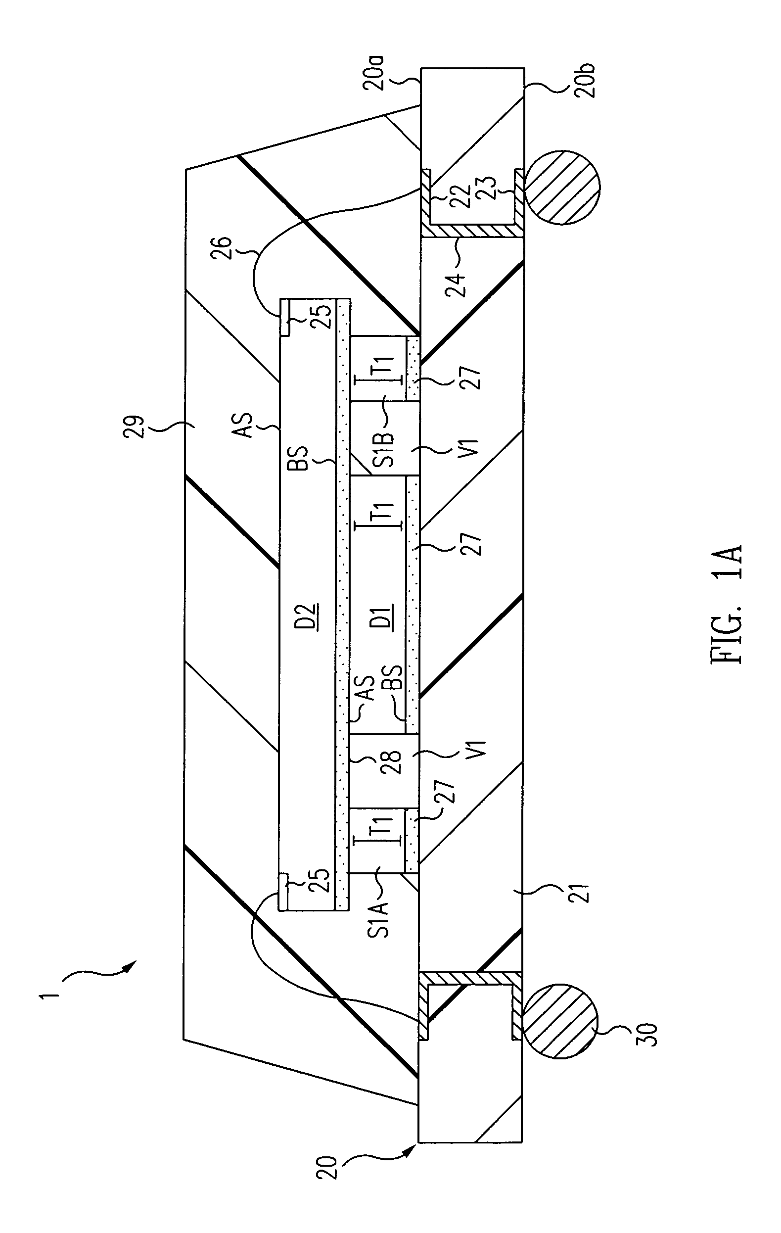
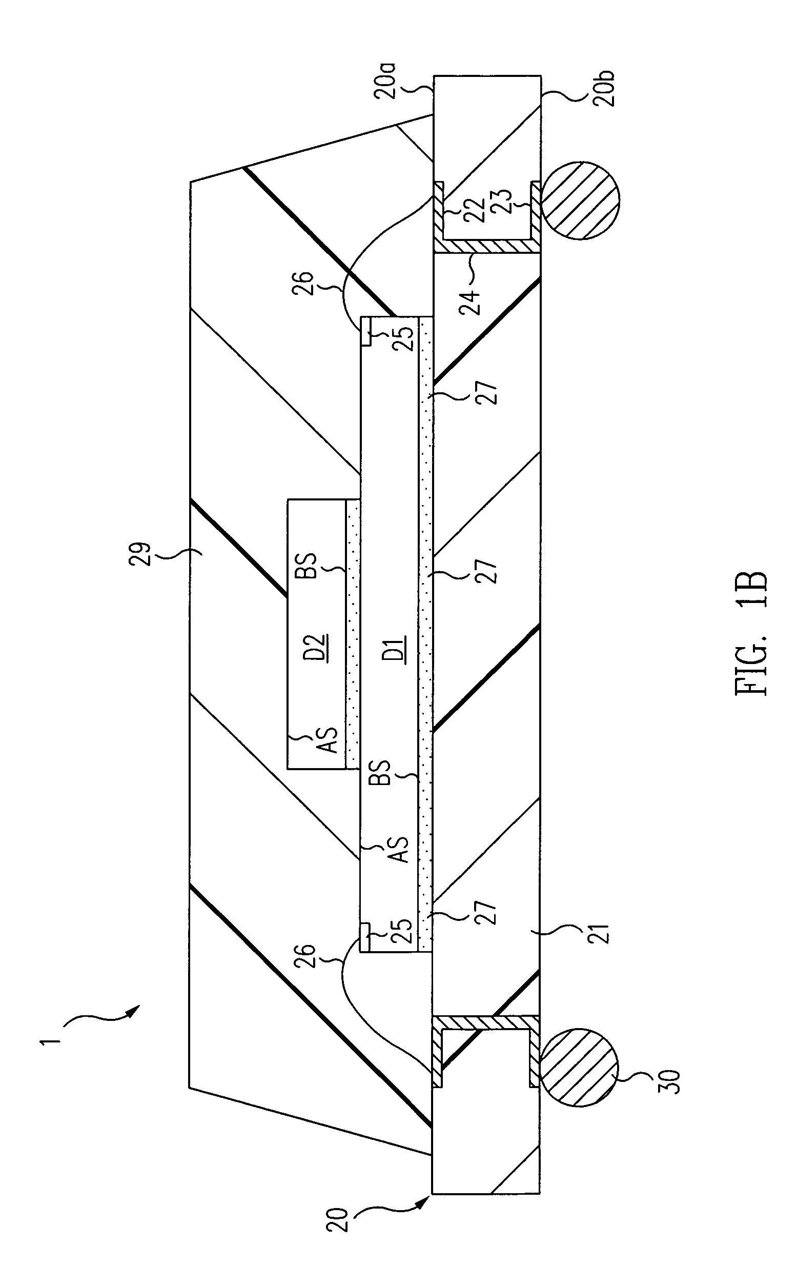
[0041]FIGS. 1A and 1B illustrate a semiconductor package 1 in accordance with the present invention. The views of FIGS. 1A and 1B are at 90 degree angles to each other. FIG. 1A is taken along line 1A—1A of FIG. 3B, and the cross-sectional side view of FIG. 1B is taken along line 1B—1B of FIG. 3B.

[0042]Semiconductor package 1 includes two semiconductor dies, labeled D1 and D2, stacked one on top of the other and coupled together by an adhesive layer 28. The upper semiconductor die D2 is supported by underlying semiconductor die D1 and two underlying supports, labeled S1A and S1B. The number “1” in the labels D1 and S1A, S1B indicates that these structures are at a first level of a semiconductor die stack relative to the substrate. The number “2” in the label D2 indicates that the structure is in the second layer of the stack relative to the substrate. The letters “A” and “B” in the labels S1A and S1B distinguish between two similar structures in the same level of the stack. We will u...

second embodiment

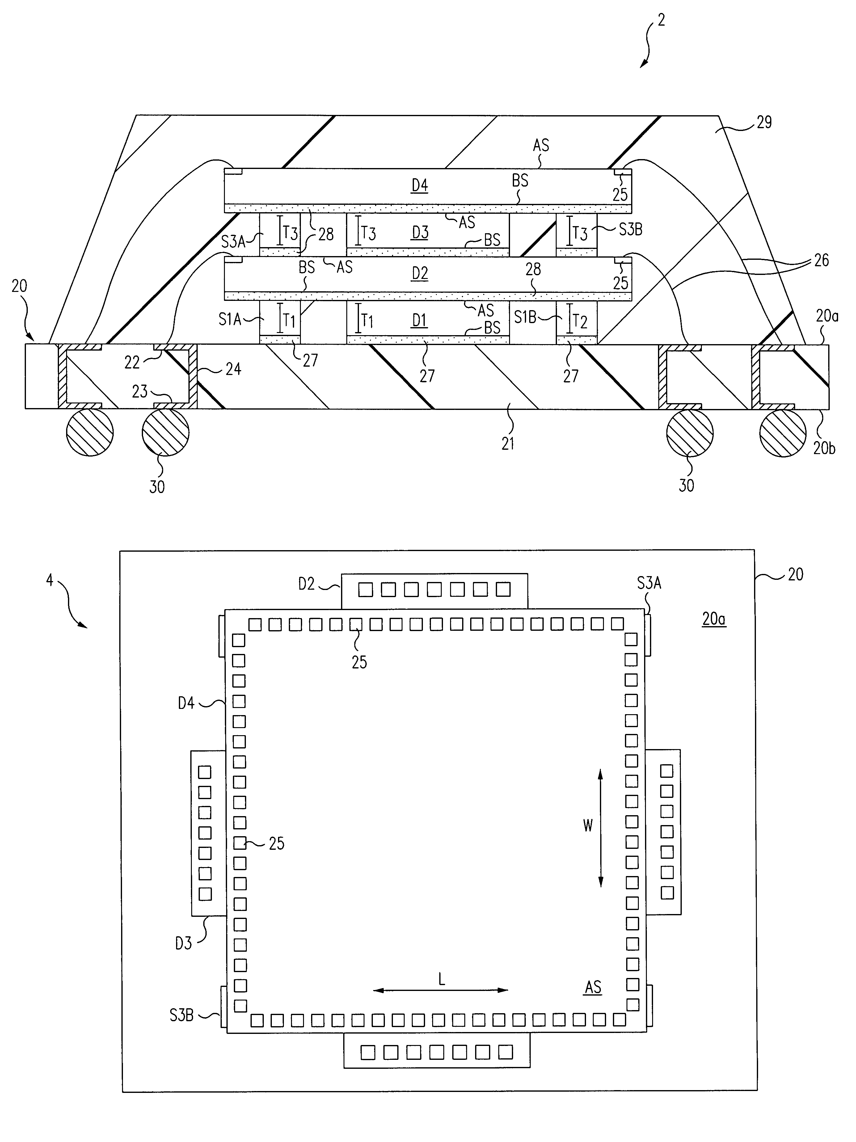
[0072]FIGS. 4A and 4B are cross-sectional side views of a semiconductor package 2 within the present invention. FIGS. 5A–5D are simplified top plan views of semiconductor package 2. The cross-sectional view of FIG. 4A is taken along line 4A—4A of FIG. 5D, and the cross-sectional view of FIG. 4B is taken along line 4B—4B of FIG. 5D, which is 90 degrees from line 4A—4A.

[0073]Semiconductor package 2 includes a stack of four same-size semiconductor dies D1, D2, D3, and D4. Many aspects of semiconductor package 2 match aspects of semiconductor package 1, such as the form of substrate 20, bond wires 26, encapsulant 29, and solder balls 30. In addition, the arrangement and stacking of the lowest two semiconductor dies D1 and D2 and supports S1A, S1B of semiconductor die 2 of FIGS. 4A, 4B, 5A, and 5B is the same as the arrangement and stacking of semiconductor dies D1 and D2 and supports S1A, S1B of semiconductor package 1 of FIGS. 1A, 1B, 3A, and 3B. Accordingly, redundant discussion may b...

third embodiment

[0087]FIGS. 6A and 6B are cross-sectional side views of a semiconductor package 3 within the present invention. FIGS. 7A–7D are simplified top plan views of semiconductor package 3. The cross-sectional view of FIG. 6A is taken along line 6A—6A of FIG. 7D, and the cross-sectional view of FIG. 6B is taken along line 6B—6B of FIG. 7D, 90 degrees from line 6A—6A. Many aspects of semiconductor package 3 are the same as in semiconductor packages 1 and 2, and hence our discussion will focus on differences between the semiconductor packages and will largely omit redundant discussion.

[0088]Semiconductor package 3 includes a stack of four semiconductor dies D1, D2, D3, and D4. Unlike the die stacks of semiconductor packages 1 and 2, however, each successive semiconductor die DN (where “N” is the stack level) above the lowermost semiconductor die D1 is supported by the immediately underlying die D(N−1)and only one immediately underlying support S(N-1), whereas in semiconductor packages 1 and 2...


PUM


Abstract

A stack of semiconductor dies is disclosed. A first stack level includes a first semiconductor die and at least one first support that are attached to a substrate surface. A second level includes a second semiconductor die and at least one second support that are attached to the active surface of the first semiconductor die and to a coplanar surface of the first support(s). A third level includes a third semiconductor die attached to the active surface of the second semiconductor die and to a coplanar surface of the second support(s). The second and third semiconductor dies do not overlap bond pads of the first and second semiconductor dies, respectively. An adhesive film overlies the entire inactive surface of the second and third semiconductor dies, and attaches the second and third semiconductor dies to the immediately underlying active surface and support(s).

Description

BACKGROUND OF THE INVENTION[0001]a. Field of the Invention[0002]The present invention is in the field of semiconductor die packaging.[0003]b. Description of the Related Art[0004]Electronic equipment that includes packaged semiconductor dies, such as portable telephones, personal computers, and digital cameras, are being developed with increased functionality. To meet this trend, companies that assemble semiconductor dies into packages are developing semiconductor packages that include a plurality of stacked semiconductor dies in a single package.[0005]A conventional technique for stacking plural semiconductor dies in a single package is to couple an inactive (i.e., backside) surface of a first semiconductor die to a substrate, so that the active surface of the first semiconductor die faces away from the substrate, and then to attach the inactive surface of a second semiconductor die onto the active surface of the first semiconductor die using an electrically insulating adhesive laye...

Claims


Application Information

Patent Timeline
Patent Type & Authority Patents(United States)
IPC IPC(8): H01L23/48H01L25/065
CPCH01L25/0657H01L2224/48091H01L2224/48227H01L2224/73265H01L2225/0651H01L2225/06555H01L2225/06562H01L2225/06575H01L2225/06582H01L2924/15311H01L2924/00014H01L2224/32145H01L2224/32225H01L2224/16225H01L2924/00012H01L2224/92247H01L2224/73204H01L2924/00H01L24/73H01L2924/14H01L2224/05571H01L2224/05573H01L2924/181H01L2224/05554H01L25/0652H01L2224/73253H01L24/05H01L2224/05599
Inventor ST. AMAND, ROGER D.PERELMAN, VLADIMIR
Owner AMKOR TECH SINGAPORE HLDG PTE LTD
Why Eureka
Try Eureka