Electronic apparatus capable of using an external power source and a bus power source simultaneously

Inactive Publication Date: 2005-08-23
BENQ CORP
5 Cites 9 Cited by

AI-Extracted Technical Summary

Problems solved by technology

The use of the USB power source makes the scanner 200 convenient for the user, but the limitations of the USB power source also make less functionality and performance of the scanner 200 than the typical scanner 100 powered by the external power source.
Since the scanner 100 uses an internal voltage converter to convert an external voltage into the necessary voltage for its internal electronic devices, heat dissipation from the voltage converter during voltage conversion would unavoidably raise the inside temperature of the scanner 100, thus resulting in thermal dri...

Benefits of technology

[0012]It is therefore an object of the invention to provide an electronic apparatus, such as a scanner, to achieve the following purposes: (1) reducing power dissipation...

Abstract

An electronic apparatus capable of using an external power source and a power source from a bus, such as a universal serial bus (USB) power source, is disclosed. The external power source and the USB power source output a first and a second operating voltage to the electronic apparatus, respectively. The electronic apparatus includes a first group of devices operative at the first operating voltage, a second group of devices operative at the second operating voltage, and an input power control circuit. The input power control circuit is coupled to the first and second groups of devices, and is capable of being coupled to the external and the USB power sources. The input power control circuit is used for controlling the first and the second operating voltages in order to feed the first and second groups of devices with the first and the second operating voltages, respectively.

Application Domain

Volume/mass flow measurementPower supply for data processing

Technology Topic

Power controlEngineering +4

Image

  • Electronic apparatus capable of using an external power source and a bus power source simultaneously
  • Electronic apparatus capable of using an external power source and a bus power source simultaneously
  • Electronic apparatus capable of using an external power source and a bus power source simultaneously

Examples

  • Experimental program(1)

Example

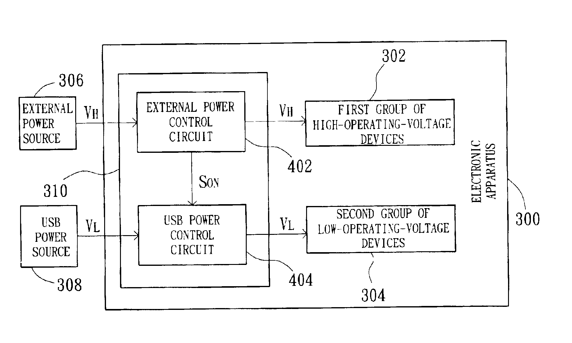
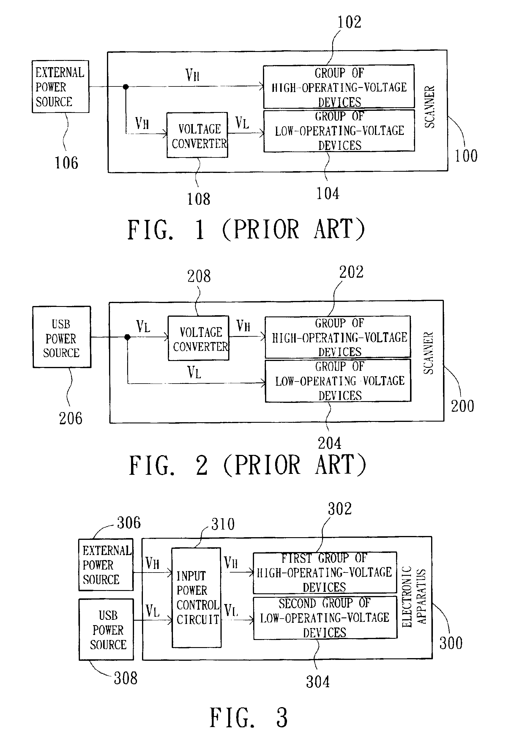
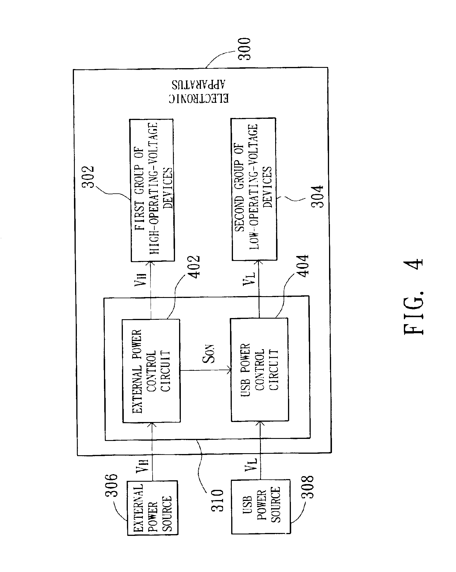
[0019]The principle of the invention is that an electronic apparatus, such as a scanner, is simultaneously coupled to an external power source supplying a high operating voltage and a power source from a bus, such as a USB power source, supplying a low operating voltage. In addition, under the control of an input power control circuit, after the high operating voltage provided by the external power source is fed to the scanner, the low operating voltage provided by the USB power source is then fed to the scanner.
[0020]As shown in FIG. 3, an electronic apparatus, such as a scanner 300, capable of using an external power source 306 and a USB power source 308, according to one preferred embodiment of the invention, is connected to the external power source 306 and the USB power source 308. As described above, the scanner 300 includes two groups of devices: a first group of high-operating-voltage devices 302, directly or indirectly operative at 12 V DC, and a second group of low-operating-voltage devices 304, directly or indirectly operative at 5 V DC. In addition, the first group of high-operating-voltage devices 302 and the second group of low-operating-voltage devices 304 are independent, such that, they are operative at their respective operating voltages. Please note that although some electronic devices may use both the operating voltages of 12 and 5 V DC simultaneously, they will not be described specifically in the following for the sake of simplicity.
[0021]In one embodiment of the present invention, the scanner 300 is coupled to the external power source 306 and the USB power source 308 simultaneously. The external power source 306 outputs a high operating voltage VH of 12 V DC, capable of supplying power to the first group of high-operating-voltage devices 302. The USB power source 308 outputs a low operating voltage VL of 5 V DC, capable of supplying power to the second group of low-operating-voltage devices 304. The scanner 300 also includes an input power control circuit 310. The input power control circuit 310 is coupled to both the first group of high-operating-voltage devices 302 and the second group low-operating-voltage devices 304. The input power control circuit 310 is capable of being coupled to the external power source 306 and the USB power source 308. The input power control circuit 310 is used for controlling the input of the high operating voltage VH and the low operating voltage VL to the first group of high-operating-voltage devices 302 and the second group of low-operating-voltage devices 304, respectively. In order to avoid unexpected operations due to feeding the low operating voltage VL or the high operating voltage VH to the scanner 300 too early, the input power control circuit 310 can determine when each of the two different operating voltages is fed. In this embodiment, the input power control circuit 310 first feeds the high operating voltage VH to the first group of high-operating-voltage devices 302 and then feeds the low operating voltage VL to the second group of low-operating-voltage devices 304.
[0022]FIG. 4 illustrates the structure of an input power control device 310. The input power control device 310 includes an external power control circuit 402 and a USB power control circuit 404. The external power control circuit 402 is coupled to the first group of high-operating-voltage devices 302 and the external power source 306. The USB power control circuit 404 is coupled to the second group of low-operating-voltage devices 304, the external power control circuit 402, and the USB power source 308. When the high operating voltage VH is fed to the input power control circuit 310, the external power control circuit 402 first feeds the high operating voltage VH to the first group of high-operating-voltage devices 302. Next, the external power control circuit 402 allows the USB power control circuit 404 to feed the low operating voltage VL to the second group of low-operating-voltage devices 304 by outputting a control signal SON to the USB power control circuit 404.
[0023]In this embodiment, the scanner 300 is coupled to the external power source 306 for providing the high operating voltage VH, and the USB power source 308 for providing the low operating voltage VL. Thus, the scanner 300 has no need for converting the input voltages into the operating voltages of electronic devices inside the scanner 300, and thus reducing unnecessary power dissipation. Accordingly, thermal drifting of the electronic devices inside the scanner 300 due to the heat dissipation generated during voltage conversion would be avoided. Therefore, signal distortion due to thermal drifting would be avoided, and the scanning quality would not be degraded.
[0024]In addition, under the control of the input power control circuit 310, the high operating voltage VH can first be fed to the first group of high-operating-voltage devices 302 and then the low operating voltage VL can be fed to the second group of low-operating-voltage devices 304. The scanner 300 is operative only when the supply of the two different operating voltages VH and VL is stabilized. Thus, damage of the internal devices of the scanner 300 due to unstable power supply can be prevented and the lifetime of the scanner 300 can be increased because the scanner 300 is operative only when the user operates the scanner 300 in a proper starting procedure.
[0025]The scanner 300 in this embodiment obtains the necessary power from the external power source 306 and the USB power source 308 simultaneously. The high operating voltage VH outputted by the external power source 306 is supplied to the first group of high-operating-voltage devices 302 only. The USB power source 308 is also an external power source, for example, a device of a personal computer. However, in terms of power efficiency, the direct use of the 5V DC provided by the USB power source 308 in the scanner 300 is more efficient than the additional converter adopted by the conventional scanners by which a 12 V DC is converted into a 5 V DC. For a personal computer, a highly efficient voltage converter is commonly used to supply a 5 V DC; on the other hand, the conventional scanner adopts a simpler voltage converter for the sake of low production cost. Thus, according to the invention, although the power dissipated by the first group of high-operating-voltage devices 302 and the second group of low-operating-voltage devices 304 of the scanner 300 remains unchanged, the scanner 300 does operate at a reduced operating temperature, and if the personal computer of the USB power source 308 is taken into account, the total energy usage efficiency is enhanced and the total energy dissipation is reduced indeed.
[0026]In addition to scanners, the principle of the invention can be applied to other electronic apparatuses. If the internal electronic devices of an electronic apparatus use two different operating voltages respectively, the electronic apparatus can use an external power source and a USB power source simultaneously as its operating power sources.
[0027]As disclosed above, the scanner that uses the external power source and the USB power source simultaneously can achieve the following advantages.
[0028]1. Thermal drifting of the internal electronic devices is decreased due to reducing power dissipation. The scanner does not need to convert the input voltage into the operating voltage for the electronic devices inside the scanner, thus reducing the power dissipation and thus, preventing thermal drifting of the internal electronic devices that would affect the operation of the scanner.
[0029]2. Undesired erroneous operations are prevented and the lifetime of the scanner is increased. Damage to the internal electronic devices of the scanner can be reduced by using the input power control circuit to ensure that the scanner is operative only if the scanner is operated through by a proper starting procedure. Thus, the decrease in damage of the internal electronic devices can result in an increase in the lifetime of the scanner.
[0030]3. An external power source can use a reduced power, and thus, power saving can be achieved. Since the high operating voltage outputted by the external power source is only applied to the first group of high-operating-voltage devices of the scanner, a reduced power is required of the external power source, thus saving power.
[0031]While the invention has been described by way of example and in terms of a preferred embodiment, it is to be understood that the invention is not limited thereto. On the contrary, it is intended to cover various modifications and similar arrangements and procedures, and the scope of the appended claims therefore should be accorded the broadest interpretation so as to encompass all such modifications and similar arrangements and procedures.

PUM

no PUM

Description & Claims & Application Information

We can also present the details of the Description, Claims and Application information to help users get a comprehensive understanding of the technical details of the patent, such as background art, summary of invention, brief description of drawings, description of embodiments, and other original content. On the other hand, users can also determine the specific scope of protection of the technology through the list of claims; as well as understand the changes in the life cycle of the technology with the presentation of the patent timeline. Login to view more.

Similar technology patents

Memory circuit, display circuit, and display device

InactiveUS7173593B2prevent degradationreduced power dissipation
Owner:ADVANCED LCD TECH DEVMENT CENT

Method for forming semiconductor device

InactiveUS20100216290A1reduced power dissipationextra cost of be save
Owner:ANPEC ELECTRONICS CORPORATION

Driver circuit for driving a print head of an inkjet printer

InactiveUS20110261097A1reduced power dissipation
Owner:OCE TECH

Adaptive Power Savings on a Device Display

InactiveUS20150061988A1reduced power dissipation
Owner:TEXAS INSTR INC

Parallel data path architecture for high energy efficiency

InactiveUS20060112258A1improve performancereduced power dissipation
Owner:ELECTRONICS & TELECOMM RES INST

Classification and recommendation of technical efficacy words

  • avoid signal distortion
  • reduced power dissipation

Semiconductor radioactive ray detector, radioactive ray detection module, and nuclear medicine diagnosis apparatus

InactiveUS20080277589A1improved electrical conductivityavoid signal distortion
Owner:HITACHI LTD

Ripple suppression circuit based audio power amplification system

InactiveCN105978497Aavoid signal distortionQuality assurance
Owner:CHENGDU NIAOER ELECTRONICS TECH CO LTD

Wireless network intelligent amplifier

InactiveCN103684305Aavoid signal distortionHigh quality and reliable transmission
Owner:方大铮

Method and device for identifying signal transmission integrity

PendingCN112951137Aavoid signal distortionavoid distortion
Owner:SHENZHEN CHINA STAR OPTOELECTRONICS SEMICON DISPLAY TECH CO LTD

Improved SLM-PTS peak average power ratio suppression method

PendingCN113347131AImprove PAPR inhibition abilityavoid signal distortion
Owner:DALIAN MARITIME UNIVERSITY

Method and apparatus for controlling a selectable voltage audio power output stage

ActiveUS20080144861A1improve efficiencyreduced power dissipation
Owner:CIRRUS LOGIC INC

Bridge-less boost (BLB) power factor correction topology controlled with one cycle control

InactiveUS20050105311A1reduced power dissipationreduce in size
Owner:INTERNATIONAL RECTIFIER COEP

Adaptive Power Savings on a Device Display

InactiveUS20150061988A1reduced power dissipation
Owner:TEXAS INSTR INC

Memory circuit, display circuit, and display device

InactiveUS7173593B2prevent degradationreduced power dissipation
Owner:ADVANCED LCD TECH DEVMENT CENT

Method for forming semiconductor device

InactiveUS20100216290A1reduced power dissipationextra cost of be save
Owner:ANPEC ELECTRONICS CORPORATION
Why Eureka
Try Eureka