
Double polysilicon bipolar transistor and method of manufacture therefor

a bipolar transistor and polysilicon technology, applied in the field of bipolar transistors, can solve the problems of difficult manufacturing of conventional bipolar transistors, large cost, and inability to improve, and achieve the effects of reducing size, improving efficiency, and consistent current driving capability

Inactive Publication Date: 2005-08-30
CHARTERED SEMICONDUCTOR MANUFACTURING
View PDF5 Cites 3 Cited by
  • Summary
  • Abstract
  • Description
  • Claims
  • Application Information

AI Technical Summary

Benefits of technology

[0019]The present invention provides a bipolar transistor, and a method of manufacturing therefor, with a substrate having a collector region and a base structure thereon. An emitter structure is formed over the base structure and an extrinsic base structure is formed over the base structure and over the collector region beside and spaced from the emitter structure. A dielectric layer is deposited over the substrate and connections are formed to the extrinsic base structure, the emitter structure and the buried collector. The bipolar transistor has faster operation, reduced size, consistent current driving capability, improved performance, and / or reduced cost over the prior art. The manufacturing method reduces the number of processing steps, provides for a smooth substrate over the intrinsic base region, reduces capacitance between the emitter and base structures, and eliminates emitter shadowing effect.

Problems solved by technology

Although a great deal of effort has been spent over the years improving bipolar transistors, they have not improved to the point where they are as popular as CMOS transistors.
The conventional bipolar transistor is difficult to manufacture and cost is a major problem.
The rough surface causes a major problem because the silicon germanium growth is irregular and its thickness is not constant as a result of the roughness.
This leads to performance problems with the device and differences from device to device.
The overlap is necessary to provide room for an emitter contact, but it causes another major problem with unwanted capacitance between the emitter and base polysilicon structures.
However, this means that variations in the size of the emitter contact will lead to a further major problem referred to as emitter shadowing effect where the size of the emitter contact cause different current gains through the emitter polysilicon structure because the emitter dopant will be implanted at different depths.
Despite many years of research and development, solutions to these problems have been long sought but have long eluded those skilled in the art.

Method used


Image

  • Double polysilicon bipolar transistor and method of manufacture therefor
  • Double polysilicon bipolar transistor and method of manufacture therefor
  • Double polysilicon bipolar transistor and method of manufacture therefor

Examples


Embodiment Construction

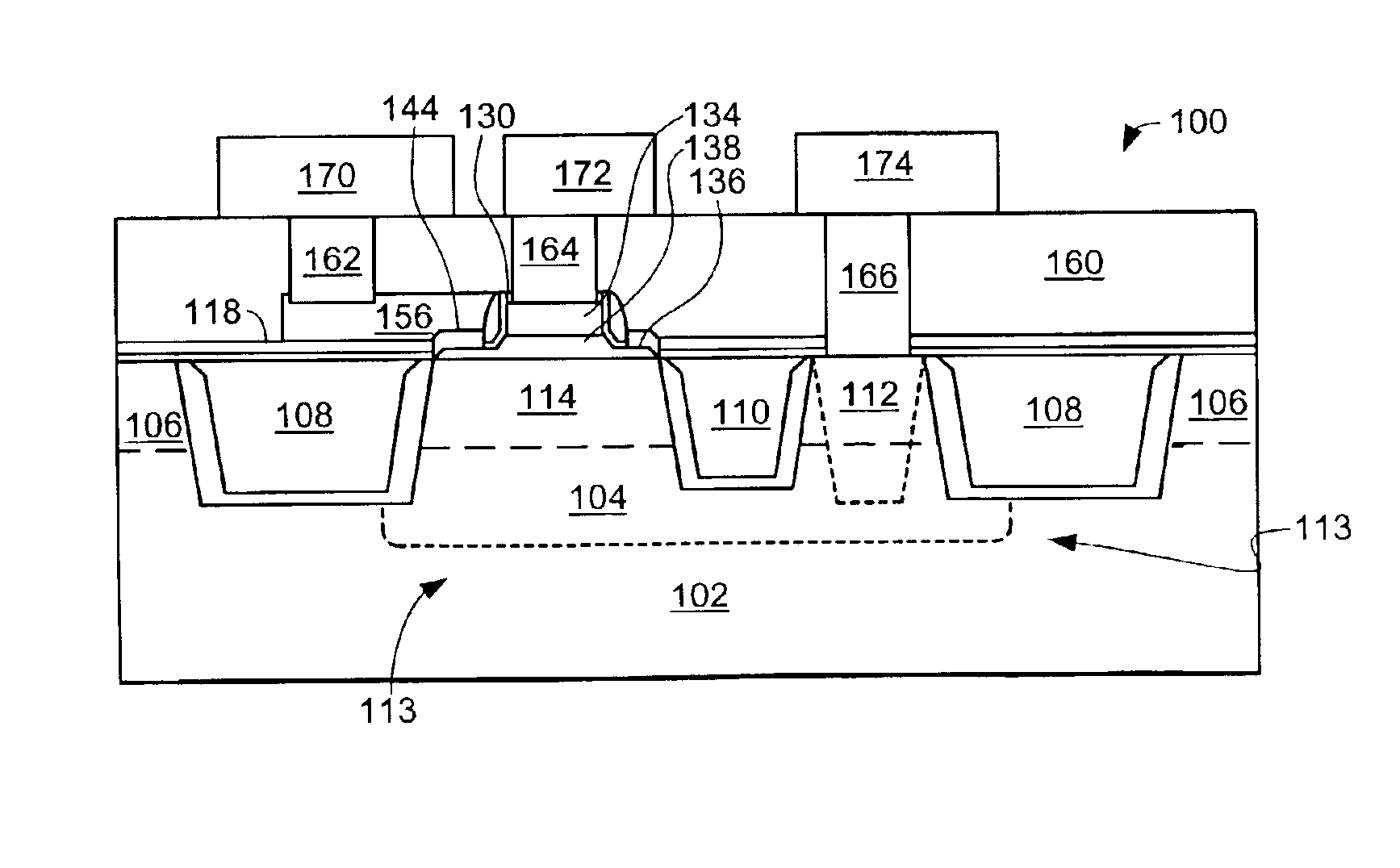
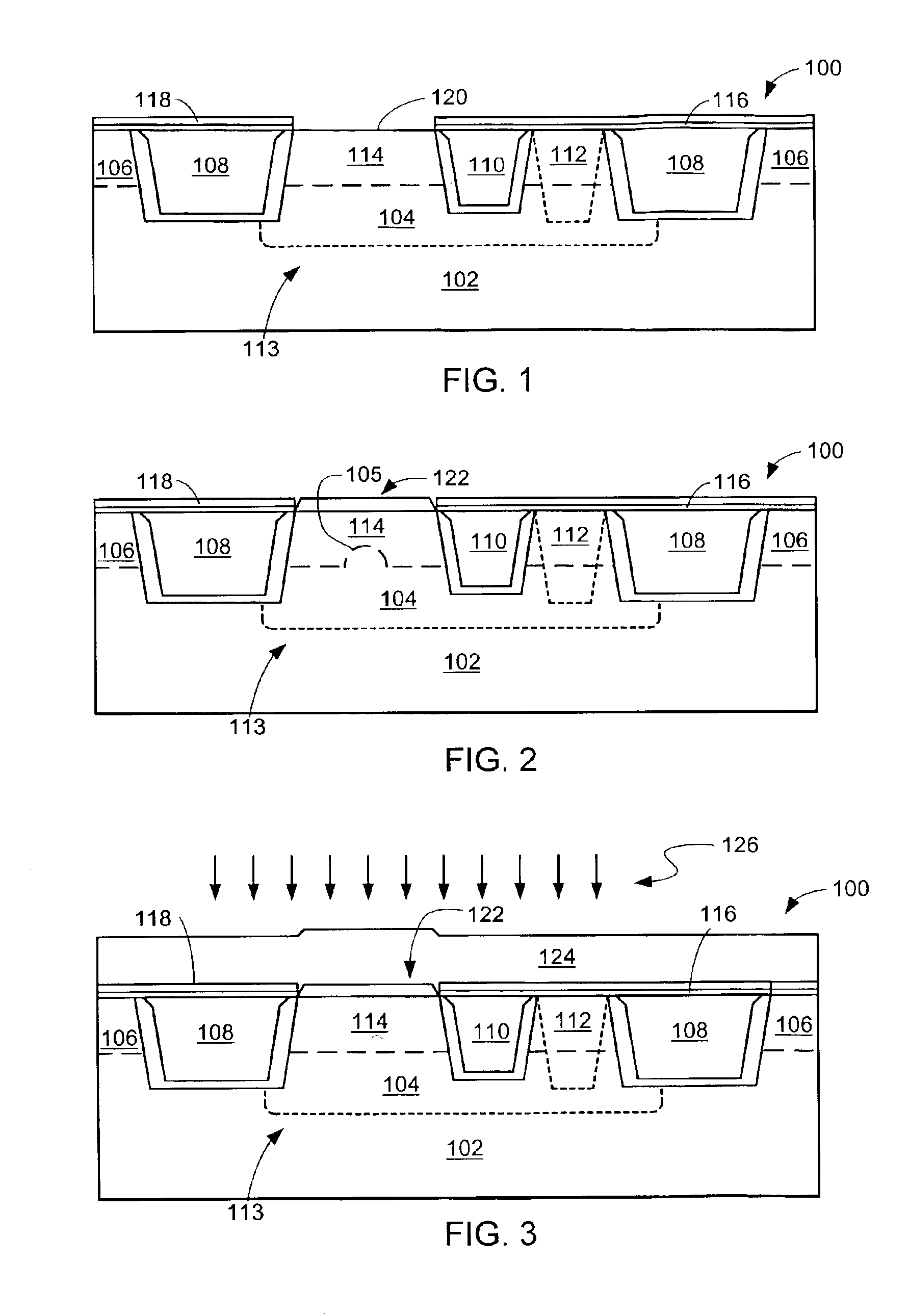
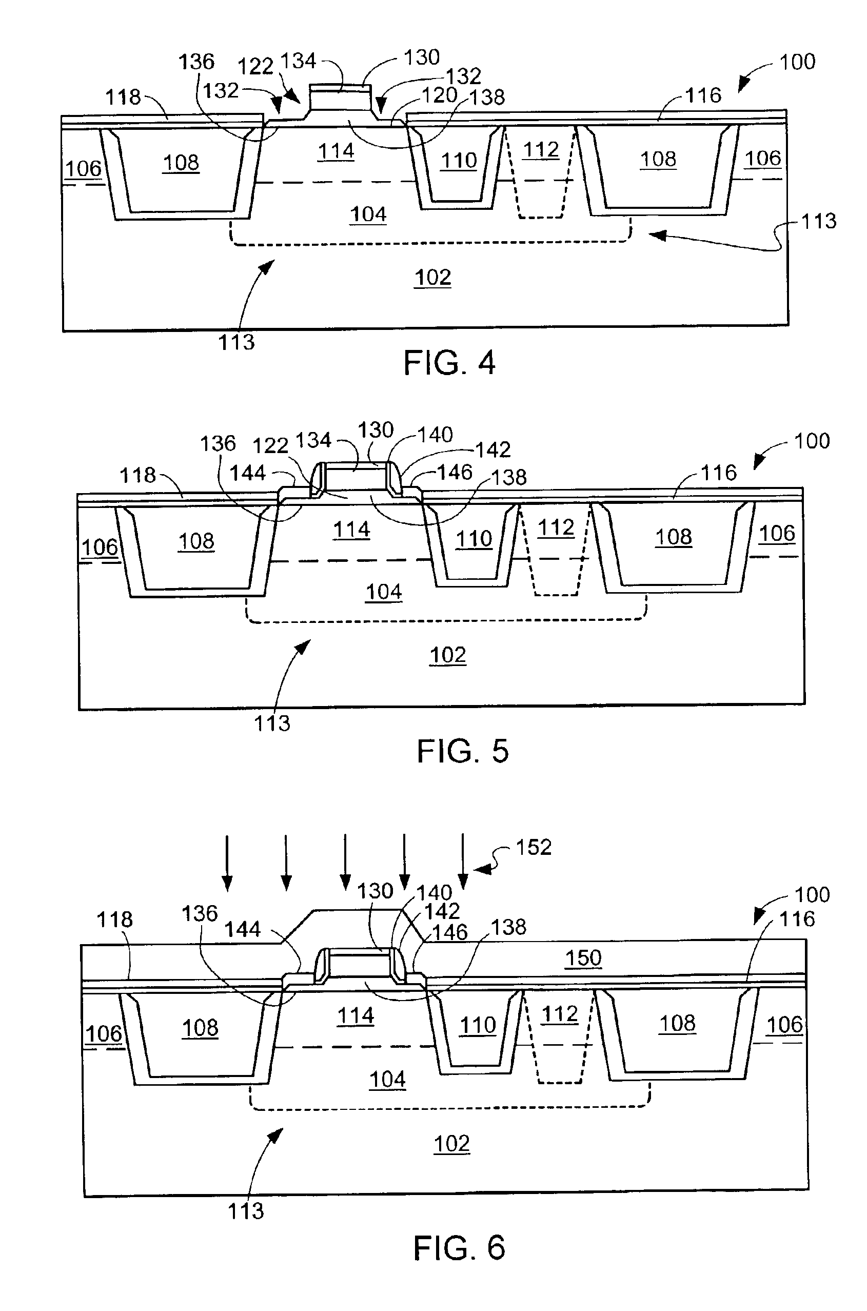
[0031]Referring now to FIG. 1, therein is shown a cross-sectional view of a bipolar transistor 100 in an intermediate stage of manufacture in accordance with the present invention. A semiconductor substrate 102 has been implanted with a dopant to form a buried collector 104. An epitaxial layer 106 of substrate material has been deposited over the semiconductor substrate 102 and the buried collector 104.

[0032]The bipolar transistor 100 has also had insulating dividers formed into the semiconductor substrate 102 and the epitaxial layer 106 that are shallow trench isolations (STI's). First and second STI's 108 and 110 are on either side of a collector tap 112, which is connected to the buried collector 104, and which is a heavily doped implant in the epitaxial layer 106. The epitaxial layer 106 on the other side from the collector tap 112 has a lower concentration of a similar type of doping as that of the buried collector 104 and forms a sub collector region 114. Collectively, the bur...


PUM


Abstract

A bipolar transistor, and manufacturing method therefor, with a substrate having a collector region and a base structure provided thereon. An emitter structure is formed over the base structure and an extrinsic base structure is formed over the base structure and over the collector region beside and spaced from the emitter structure. A dielectric layer is deposited over the substrate and connections are formed to the extrinsic base structure, the emitter structure and the collector region.

Description

BACKGROUND[0001]1. Technical Field[0002]The present invention relates generally to bipolar transistors and more specifically to double polysilicon bipolar transistors.[0003]2. Background Art[0004]Bipolar transistors were originally developed many years ago but were generally superceded by CMOS transistors, which consume less power and are less difficult to manufacture, and thus less expensive. Although a great deal of effort has been spent over the years improving bipolar transistors, they have not improved to the point where they are as popular as CMOS transistors.[0005]Recently, demand for bipolar transistors has increased significantly because these transistors are capable of operating at higher speeds and driving more current than CMOS transistors. These characteristics are important for high-speed, high frequency communication networks such as those required by cell phones and computers.[0006]Most bipolar transistors in use today are the so-called “double poly” bipolar transist...

Claims


Application Information

Patent Timeline
Patent Type & Authority Patents(United States)
IPC IPC(8): H01L21/02H01L21/331H01L29/737H01L29/732H01L29/08H01L29/02H01L29/66
CPCH01L29/0804H01L29/0821H01L29/66287H01L29/732H01L29/7375
Inventor VERMA, PURAKH RAJCHU, SHAO-FU SANFORD
Owner CHARTERED SEMICONDUCTOR MANUFACTURING
Learn More