Method and device for driving plasma display panel
a plasma display panel and plasma technology, applied in the direction of instruments, static indicating devices, etc., can solve the problems of shortening the pulse width and requiring a long time for initialization
- Summary
- Abstract
- Description
- Claims
- Application Information
AI Technical Summary
Benefits of technology
Problems solved by technology
Method used
Image

Examples
first example
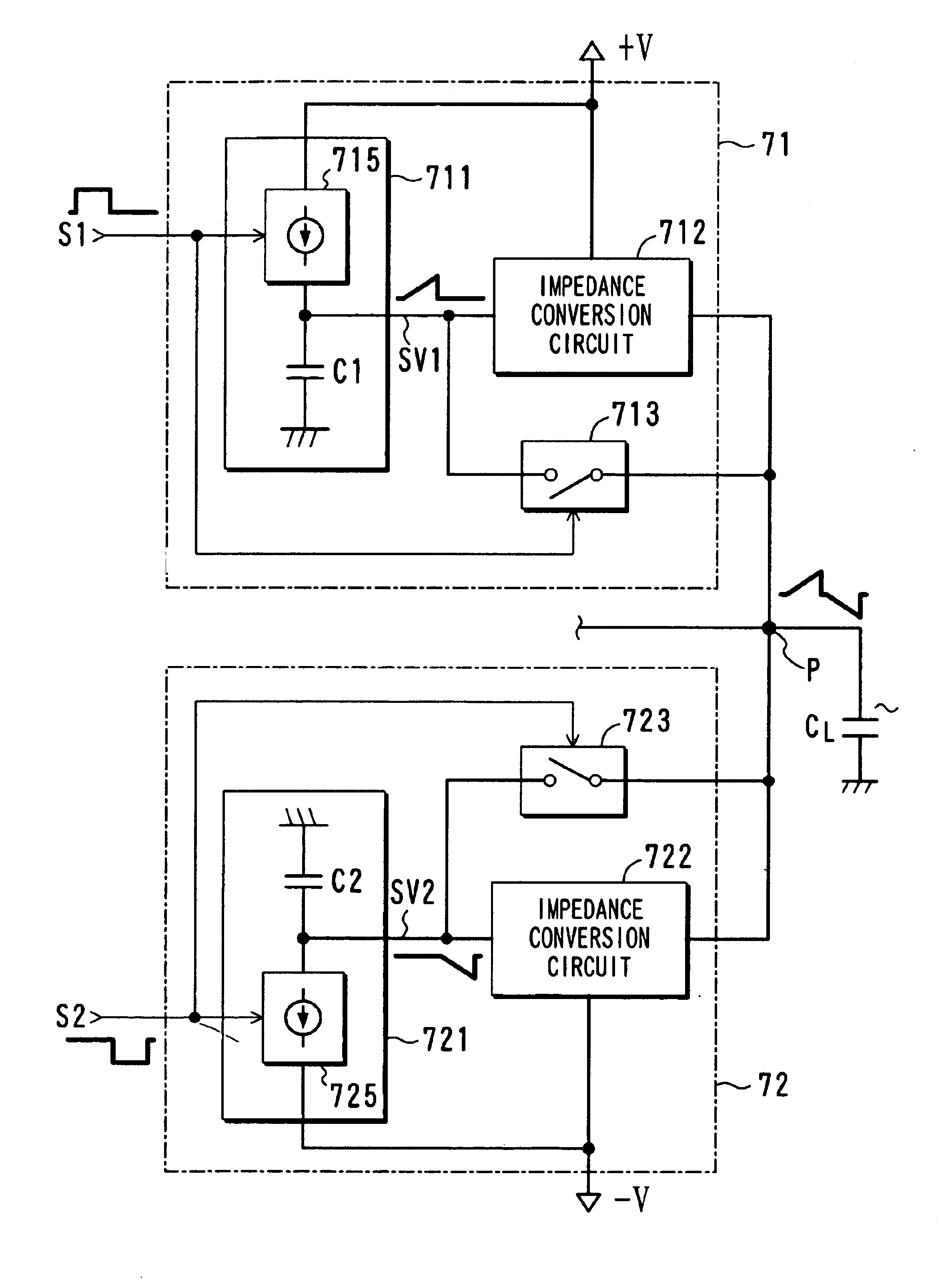
[0062]FIG. 6 is a functional block diagram of a voltage output block pair according to a first example. The positive voltage output block 71 includes a waveform generation circuit 711 for outputting an increasing voltage signal SV1 when a control signal S1 is active, an impedance conversion circuit 712 for reducing an output impedance of the waveform generation circuit 711, and a switch circuit 713 for connecting the input terminal and the output terminal of the impedance conversion circuit 712 when the control signal S1 is not active. The waveform generation circuit 711 includes a capacitance element C1 and a constant-current source 715, so as to generate an increasing voltage waveform by supplying current to the capacitance element C1. In the same way, the negative voltage output block 72 includes a waveform generation circuit 721, an impedance conversion circuit 722 and a switch circuit 723. The waveform generation circuit 721 includes a capacitance element C2 and a constant-curr...
second example
[0074]FIG. 9 is a schematic diagram of a voltage output block pair according to a second example. The second example of the positive voltage output block 71b and the negative voltage output block 72b has a feature that the impedance conversion circuits 712b and 722b include plural transistors in Darlington connection.
[0075]The above-mentioned first example has a sufficient capacity for a driving circuit of a small size panel having a small load CL whose total sum of current value due to microdischarge and the ramp waveform is less than a few ten milliamperes. However, there is a problem when driving a large size PDP of 42 inches or more whose total sum of current reaches a few hundred milliamperes. Namely, as the current increases, a variation of the gradient with respect to the output current increases. This phenomenon is caused by a base current of the impedance conversion circuit. Supposing that the output current of the impedance conversion circuit is Ic, the current of Ib=Ic / hF...
third example
[0079]FIG. 10 is a schematic diagram of a voltage output block pair according to a third example. In the third example, the positive voltage output block 71c and the negative voltage output block 72c have a feature that the impedance conversion circuits 712c and 722c include field-effect transistors Q12 and Q16 constituting a source follower. The problem of blunting the waveform in the first example is caused by the base current of the bipolar transistor. When the field-effect transistors Q12 and Q16, which are voltage control elements, are used for making the impedance conversion circuits 712c and 722c, the problem caused by the base current can be solved.
[0080]In the third example, a ramp waveform generated by charging the capacitance element C1 is supplied to the gate of the transistors Q12 and Q16. A ramp waveform output having a low impedance can be generated at the sources of the transistors Q12 and Q16 in drain connection. Differently from the first example and the second exa...
PUM
 Abstract
Description
Claims
Application Information
PatSnap Eureka turns technology decisions into work you can execute. Powered by our Innovation Knowledge Graph, it runs expert workflows across engineering, life sciences, materials and intellectual property. Get your review-ready output in minutes.


