Structure and method of forming a bipolar transistor having a void between emitter and extrinsic base

Inactive Publication Date: 2005-09-06
GLOBALFOUNDRIES INC
View PDF12 Cites 48 Cited by
  • Summary
  • Abstract
  • Description
  • Claims
  • Application Information

AI Technical Summary

Problems solved by technology

Although these capacitances impact the power gain of the transistor, they are an inextricable part of the ideal transistor structure and thus cannot be fully eliminated.
A problem of the non-self-aligned structure of HBT 10 is high base resistance Rb.
A drawback of this method is that the extrinsic base layer thickness, hence the base r

Method used


Image

  • Structure and method of forming a bipolar transistor having a void between emitter and extrinsic base
  • Structure and method of forming a bipolar transistor having a void between emitter and extrinsic base
  • Structure and method of forming a bipolar transistor having a void between emitter and extrinsic base

Examples


Embodiment Construction

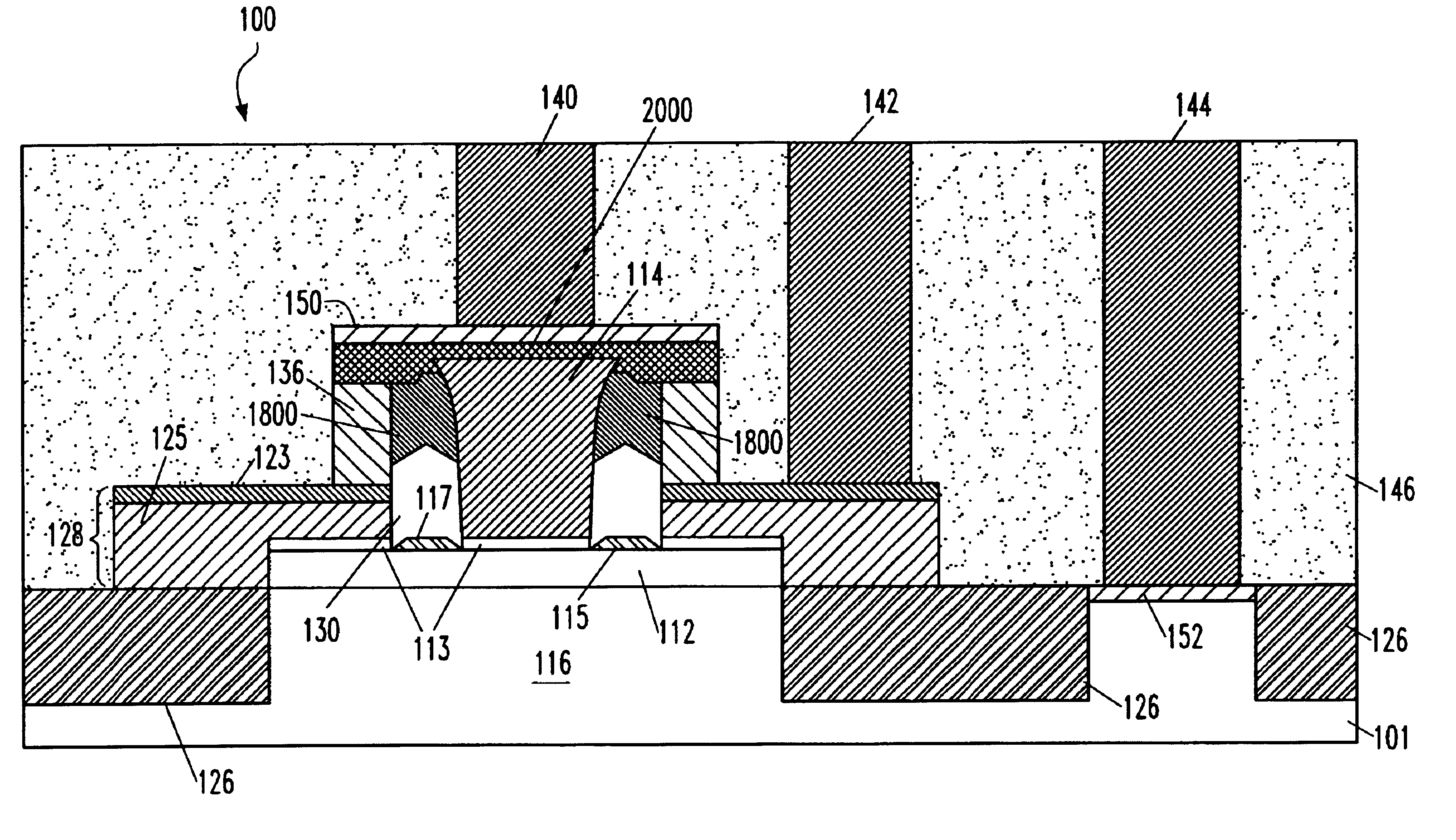
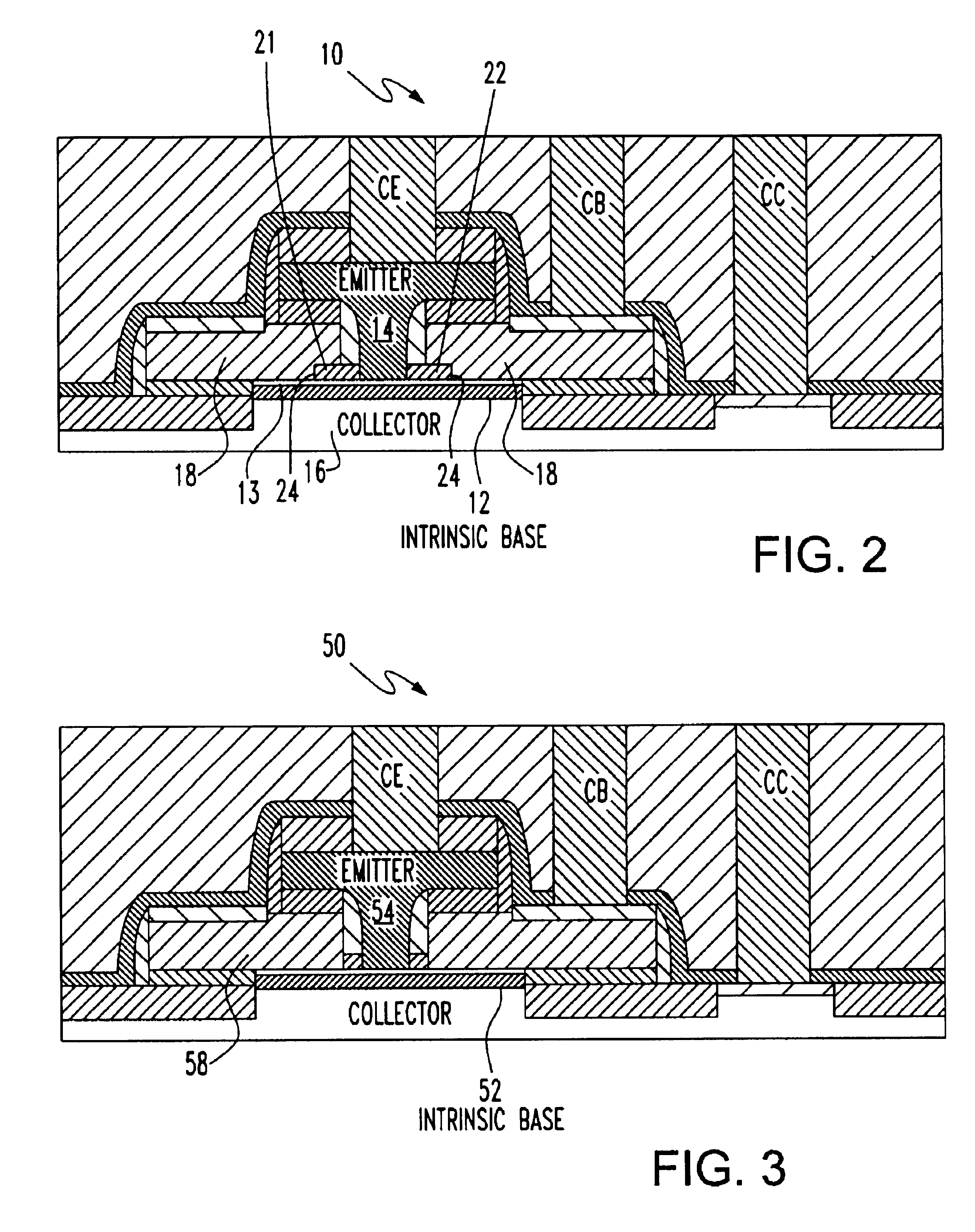
[0033]The embodiments of the invention described herein provide a structure and method for forming a bipolar transistor having reduced collector-base capacitance (C cb). Reducing the collector-base capacitance affects the power gain of the transistor, helping to increase fT and fMAX, According to the embodiments of the invention, these goals are furthered without significant impact to series resistance (Rc) or base resistance (Rb), thus enabling improvements to be achieved in the gain and frequency range of a bipolar transistor.

[0034]The bipolar transistor according to the various embodiments described herein includes an “air gap”, i.e. a gap filled with any suitable one or combination of gases or a vacuum void (hereinafter “gap”) in the place of a traditional solid dielectric spacer of silicon nitride or silicon dioxide between the emitter and the raised extrinsic base. The use of a gap in place of such solid dielectric reduces the dielectric constant by a 3:1 ratio or greater and ...


PUM


Abstract

Structure and a method are provided for making a bipolar transistor, the bipolar transistor including a collector, an intrinsic base overlying the collector, an emitter overlying the intrinsic base, and an extrinsic base spaced from the emitter by a gap, the gap including at least one of an air gap and a vacuum void.

Description

BACKGROUND OF INVENTION[0001]The present invention relates to bipolar transistors and their fabrication, especially heterojunction bipolar transistors utilized in high-speed integrated circuits.[0002]High performance circuits, especially those used for radio frequency chips, favor the use of heterojunction bipolar transistors (HBTs) to provide high maximum oscillation frequency fMAX and high transient frequency fT, also referred to as “cutoff frequency”. HBTs have a structure in which the base of the transistor includes a relatively thin layer of single-crystal semiconductor alloy material. As an example, an HBT fabricated on a substrate of single-crystal silicon can have a single-crystal base formed of silicon germanium (SiGe) having substantial germanium content and profile to improve high-speed performance. Such HBT is commonly referred to as a SIGe HBT.[0003]A particularly advantageous type of HBT has a “graded base” in which the content of particular semiconductor materials var...

Claims


Application Information

Patent Timeline
IPC IPC(8): H01L21/331H01L21/02H01L31/06H01L31/072H01L27/082H01L27/06H01L29/06H01L29/737
CPCH01L29/0649H01L29/66242H01L29/7378H01L27/0623
Inventor DIVAKARUNI, RAMAFREEMAN, GREGORYKHATER, MARWANTONTI, WILLIAM
Owner GLOBALFOUNDRIES INC
Why Eureka
Try Eureka