Multilayered chip capacitor

a multi-layer chip capacitor and capacitor technology, applied in the direction of capacitors, fixed capacitor details, fixed capacitors, etc., can solve the problems of insufficient esl reduction effect of the above-described multi-layer chip capacitor, and it is difficult to design the internal electrodes of the multi-layered chip capacitor based on desirable conditions, so as to reduce esl

Inactive Publication Date: 2005-09-06
SAMSUNG ELECTRO MECHANICS CO LTD
View PDF7 Cites 55 Cited by
  • Summary
  • Abstract
  • Description
  • Claims
  • Application Information

AI Technical Summary

Benefits of technology

[0014]Therefore, the present invention has been made in view of the above problems, and it is an object of the present invention to provide a multilayered chip capacitor, in which opened regions having simple shapes are formed in internal electrode areas so that current routes are precisely defined, thereby reducing ESL and being advantageous in terms of a design and a manufacturing process.

Problems solved by technology

However, the above-described multilayered chip capacitor cannot have sufficient ESL reduction effects.
Accordingly, it is difficult to properly design internal electrodes of a multilayered chip capacitor based on desirable characteristics of the capacitor.

Method used


Image

  • Multilayered chip capacitor
  • Multilayered chip capacitor
  • Multilayered chip capacitor

Examples


Embodiment Construction

[0030]Now, preferred embodiments of the present invention will be described in detail with reference to the annexed drawings.

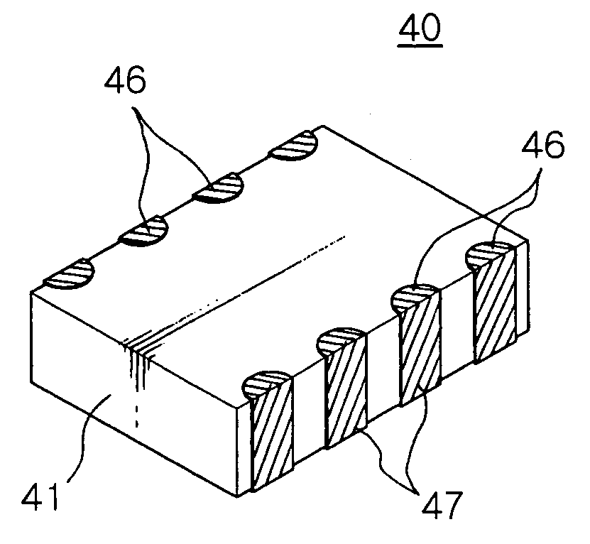
[0031]FIGS. 3a and 3b are plan views of first and second internal electrodes 32 and 33 employed by a multilayered chip capacitor in accordance with the present invention.

[0032]With reference to FIG. 3a, the first and second internal electrodes 32 and 33 are respectively formed on two dielectric layers 31a and 31b. Here, the dielectric layers 31a and 31b are neighboring two dielectric layers of a plurality of dielectric layers constituting a main body of the multilayered chip capacitor in accordance with a preferred embodiment of the present invention.

[0033]As shown in FIG. 3a, the first internal electrode 32 formed on one dielectric layer 31a includes a lead 34 extended from one side thereof, and the second internal electrode 33 formed on the other dielectric layer 31b includes a lead 35 extended from one side surface thereof facing the side surface of the fir...


PUM


Abstract

A multilayered chip capacitor including a capacitor main body including a plurality of dielectric layers, which are laminated; at least one pair of first and second internal electrodes, each of which is formed on the corresponding one of the plural dielectric layers and includes at least one lead extended to one end of the corresponding dielectric layer; a plurality of external terminals formed on the outer surface of the capacitor main body, and respectively connected to the first and second internal electrodes through the leads; and at least one opened region, formed through the inner area of each of the first and second internal electrodes, for branching the flow of current so as to increase the offset quantity of parasitic inductances between the first and second internal electrodes.

Description

RELATED APPLICATIONS[0001]The present application is based on, and claims priority from, Korean Application No. 2004-71615, filed on Sep. 8, 2004, the disclosure of which is incorporated by reference herein in its entirety.BACKGROUND OF THE INVENTION[0002]1. Field of the Invention[0003]The present invention relates to a multilayered chip capacitor, and more particularly to a multilayered chip capacitor having a low equivalent series inductance (ESL), which is properly used as a decoupling capacitor in a high frequency circuit.[0004]2. Description of the Related Art[0005]Generally, a multilayered chip capacitor (MLCC) has a structure such that internal electrodes are inserted between a plurality of dielectric layers. Such a multilayered chip capacitor has a small size and a high capacity, and is easily mounted, thus being widely used as a component of various electronic devices. Particularly, the multilayered chip capacitor serves as a decoupling capacitor, which is electrically conn...

Claims


Application Information

Patent Timeline
Patent Type & Authority Patents(United States)
IPC IPC(8): H01G4/30H01G4/232
CPCH01G4/232H01G4/30
Inventor LEE, BYOUNG HWAPARK, DONG SEOKSHIM, CHANG HOONPARK, SANG SOOPARK, MIN CHEOL
Owner SAMSUNG ELECTRO MECHANICS CO LTD
Why Eureka
Try Eureka