Device transferring method, device arraying method, and image display fabrication method using the same

a technology of device array and transfer method, which is applied in the directions of identification means, instruments, transportation and packaging, etc., can solve the problems of not being able to adapt to arraying a large number of devices, requiring a long time, and long time for the devices, so as to facilitate the transfer facilitate the re-array of a number of devices, and the effect of enlarged spa

Inactive Publication Date: 2005-09-13
SONY CORP
View PDF50 Cites 19 Cited by
  • Summary
  • Abstract
  • Description
  • Claims
  • Application Information

AI Technical Summary

Benefits of technology

[0005]A first advantage of the present invention is, therefore, to provide a device transferring method capable of readily transferring a number of devices such that the devices are enlargedly spaced from each other.
[0006]A second advantage of the present invention is to provide a device arraying method capable of readily re-arraying a number of devices such that the devices are enlargedly spaced from each other.
[0007]A third advantage of the present invention is to provide an image display unit fabrication method capable of simply fabricating an image display unit including light emitting devices arrayed in a matrix by using a device transferring method and a device arraying method according to the present invention.
[0008]According to an embodiment of the present invention, a device transferring method is provided. The method includes the step of selectively transferring part of a number of devices formed in an array on a first substrate to a flexible second substrate including an adhesive layer.
[0009]With this configuration, the devices formed in an array on the first substrate are transferred to the flexible second substrate including the adhesive layer, and accordingly, upon transfer of the devices, the flexible second substrate can be flexed along the shape of each of the devices, so that the transfer of the devices can be performed in the state that the second substrate is certainly in contact with the devices. As a result, the devices can be efficiently transferred with a high yield and a high reliability.
[0010]According to another embodiment of the present invention, a device arraying method of re-arraying a number of devices arrayed on a first substrate to a second substrate is provided. The method includes a first transfer step of transferring and holding the devices to and on a first temporarily holding member such that the devices are spaced from each other with a pitch larger than an array pitch of the devices arrayed on the first substrate. Further, the method includes a resin-covering step of covering the devices held on the first temporarily holding member with a resin, and curing the resin, a dicing step of dicing the resin to isolate the devices from each other, and a second transfer step of transferring the resin-covered devices held on the first temporarily holding member to the second substrate such that the resin-covered devices are spaced from each other with a pitch larger than an array pitch of the resin-covered devices held on the first temporarily holding member. In this method, the second transfer step further includes the steps of selectively transferring part of the number of resin-covered devices held on the first temporarily holding member to a flexible third substrate including an adhesive layer, and transferring the part of the resin-covered devices, which have been transferred to the third substrate, to the second substrate including another adhesive layer.

Problems solved by technology

This method, however, requires the step of transferring and mounting the devices one by one, and is not appropriate for arraying a large number of devices.
Such a method, however, has disadvantages in that a number of devices larger than that of the recesses must be prepared and it takes a long time for the devices to be put in the recesses, thereby requiring a long time until the device arraying step is completed.
These disadvantages are amplified when smoothly arraying devices on a substrate.

Method used


Image

  • Device transferring method, device arraying method, and image display fabrication method using the same
  • Device transferring method, device arraying method, and image display fabrication method using the same
  • Device transferring method, device arraying method, and image display fabrication method using the same

Examples


Embodiment Construction

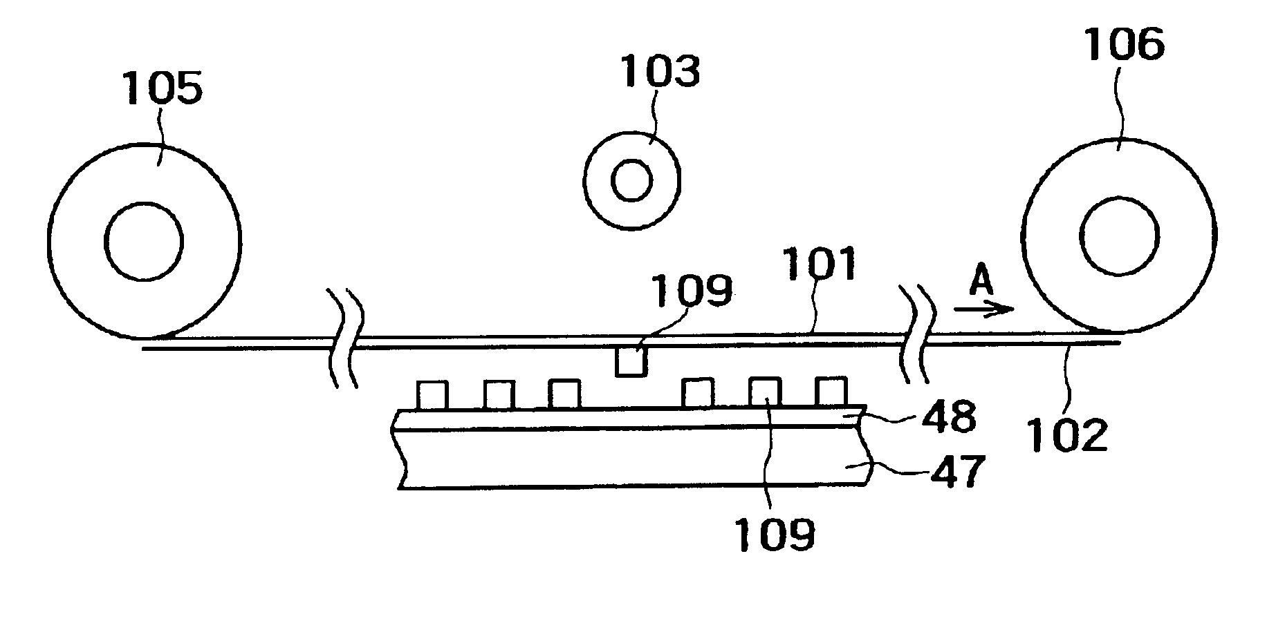
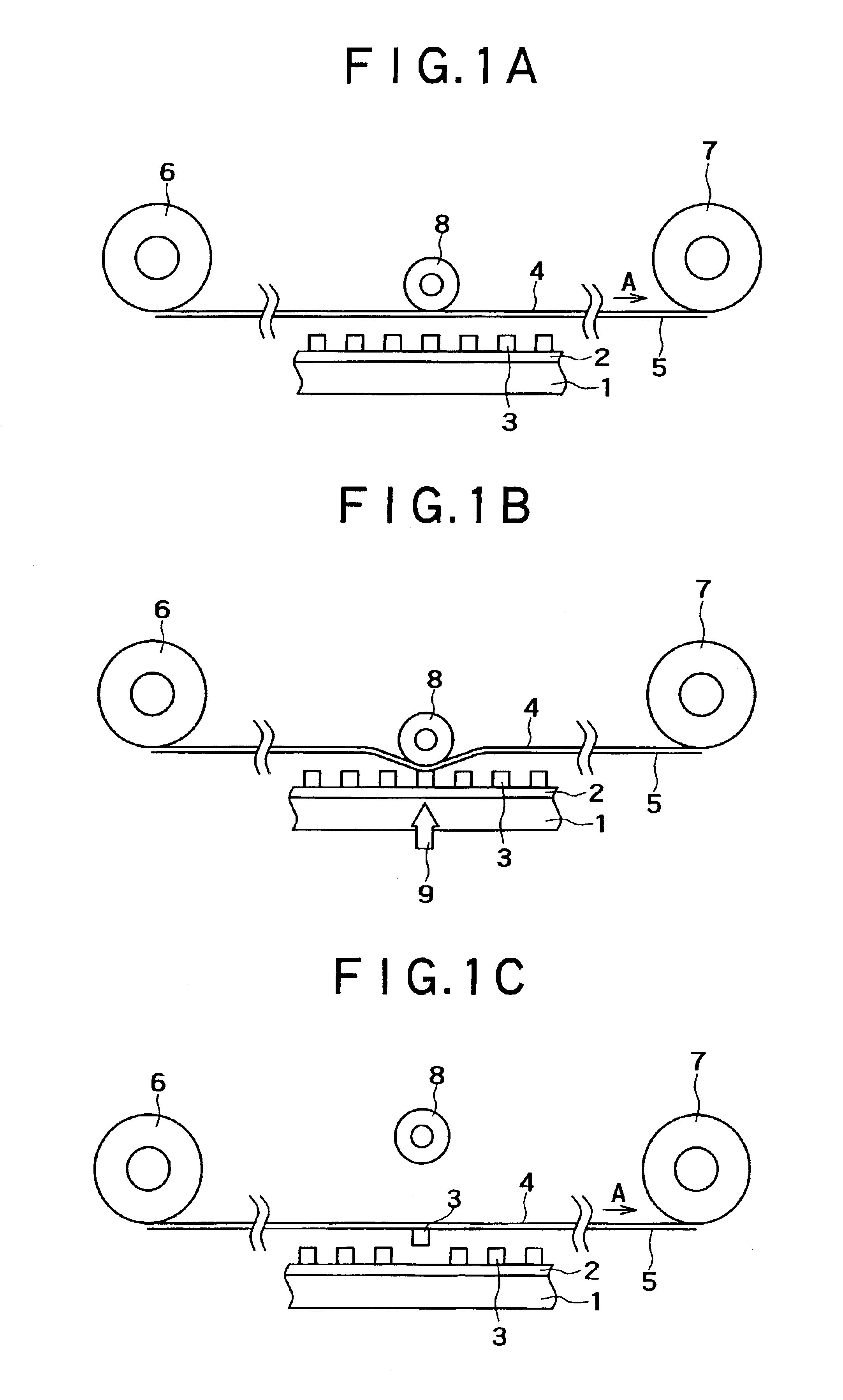
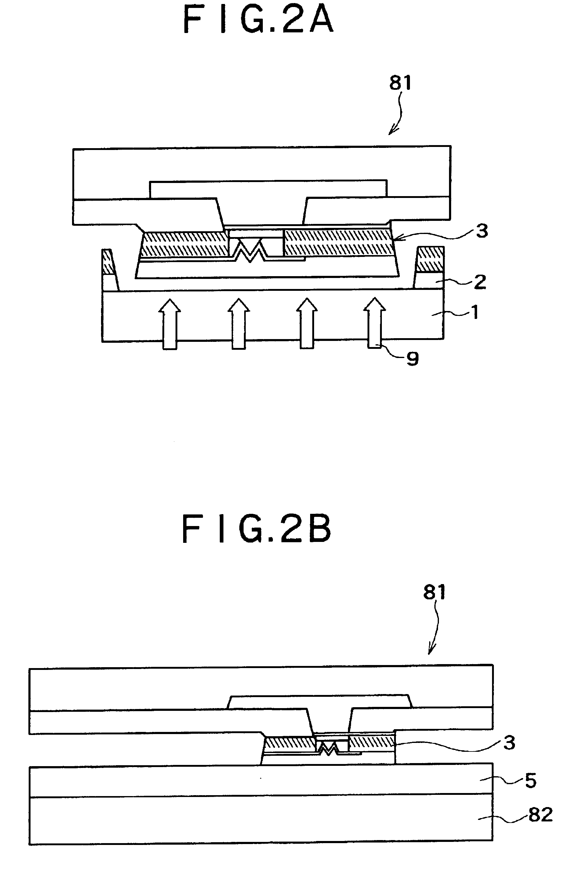
[0033]A device transferring method according the present invention, will be first described by way of an embodiment shown in FIGS. 1A to FIG. 1C. In this embodiment, the device transferring method of the present invention is applied to transfer devices formed on a base substrate to a flexible substrate.

[0034]First, as shown in FIG. 1A, an adhesive layer 2 is formed on a base substrate 1 as a supply source, and a number of devices 3 are formed in an array on the base substrate 1.

[0035]The base substrate 1 is not particularly limited but may be made from any suitable material in consideration of a combination with the devices 3, and the like.

[0036]The adhesive layer 2 may be configured as an adhesive layer allowing the devices 3 to be adhesively fixed thereto at the time of forming the devices 3 in an array on the base substrate 1 and to be later peeled therefrom at the time of picking up the devices 3 from the base substrate 1. By forming the adhesive layer 2 on the base substrate 1 ...


PUM


Abstract

A device transferring method and a device arraying method are provided for readily transferring a number of devices from a first substrate to a second substrate such that the devices are enlargedly spaced from each other with a pitch larger than an array pitch of the devices arrayed on the first substrate.

Description

BACKGROUND OF THE INVENTION[0001]The present invention relates to a device transferring method of transferring devices such as semiconductor light emitting devices, a device arraying method of re-arraying devices, each having a fine structure, densely arrayed such that the devices are enlargedly spaced from each other by making use of the device transferring method, and an image display unit fabrication method making use of the device arraying method.[0002]Methods of transferring or arraying devices are known. One of these methods involves dicing a wafer to isolate devices from each other, transferring the isolated devices from a dicing sheet to a chip tray, and picking up the devices (for example, semiconductor chips) from the chip tray by vacuum attraction to mount or connect the devices to a substrate. This method is generally carried out during a process of fabricating semiconductor packages. This method, however, requires the step of transferring and mounting the devices one by...

Claims


Application Information

Patent Timeline
Patent Type & Authority Patents(United States)
IPC IPC(8): B44C1/00B44C1/10H01L21/00H01L23/12G09F9/00H01L21/52H01L21/60H01L33/32H01L33/40H01L33/48
CPCB44C1/105H01L21/67132H01L24/24H01L24/82H01L2221/68354H01L2221/68363H01L2221/68368H01L2224/24225H01L2224/7665H01L2924/01004H01L2924/01012H01L2924/01013H01L2924/01015H01L2924/01039H01L2924/01046H01L2924/01075H01L2924/01078H01L2924/01079H01L2924/3025H01L2224/16225H01L2224/32225H01L2224/73204H01L2924/01005H01L2924/01006H01L2924/01024H01L2924/01033H01L2924/014H01L2924/00H01L2924/12041H01L21/6835H01L24/83H01L2221/68322H01L2221/68381H01L2224/05548H01L2224/05568H01L2224/05573H01L2224/73267H01L2224/92244H01L2924/12042
Inventor YANAGISAWA, YOSHIYUKIIWAFUCHI, TOSHIAKIMINAMI, MASARUHAYASHI, KUNIHIKO
Owner SONY CORP
Why Eureka
Try Eureka