Electronic circuit device including metallic member having installation members

a technology of electronic circuit device and installation member, which is applied in the direction of coupling protective earth/shielding arrangement, basic electric elements, manufacturing tools, etc., can solve the problems of reducing the resistance of wiring, unable to reduce the wiring resistance, and unable to cope with the decrease of on-state resistance, etc., to achieve small size and stably dissipate

Inactive Publication Date: 2005-09-13
PANASONIC CORP
View PDF28 Cites 27 Cited by
  • Summary
  • Abstract
  • Description
  • Claims
  • Application Information

AI Technical Summary

Benefits of technology

[0015]The present invention is devised to solve the above problems and has for its essential object to provide an electronic circuit device which is compact, has good heat radiation efficiency and can reduce resistance and stray inductance, and provide a method for manufacturing the electronic circuit device.
[0042]As described hereinabove, the electronic circuit device according to the first aspect of the the present invention is provided with the metallic wire for directly electrically connecting the second electrode formed on the other of the opposite faces of the semiconductor element and the second circuit board arranged on the side of the other opposite face. Since the conventional dented connector and projecting connector can be eliminated, the electronic circuit device can be made compact.
[0045]When the metallic wire is extended in the thickness direction of the semiconductor element and is further provided with the second bend portion, not only miniaturizing the electronic circuit device and absorbing expansion and contraction can both be achieved, but the first circuit board can be pressed against the heat radiation plate, so that heat can be stably removed.
[0046]In the electronic circuit device according to the second aspect of the present invention, the semiconductor element! is provided with the bumps on the second electrodes and metallic member having installation members, so that wiring lines are eliminated. Consequently, stray inductance and conduction resistance resulting from wiring lines can be reduced.
[0048]Since the semiconductor element and the second circuit board can be directly electically connected to each other by providing the metallic member, the conventional dented connector and projecting connector are eliminated, thus making the electronic circuit device small in size. When the heat radiation member is provided to support the second circuit board, heat from the metallic member can be stably dissipated by the one heat radiation member.
[0049]According to the manufacturing method for the electronic circuit device in the third aspect of the present invention, the solder between the semiconductor element and the metallic member is solidified after the semiconductor element and the metallic member are relatively pressed against each other so as to remove bubbles from inside the solder. Therefore, thermal conduction from the semiconductor element to the metallic member will not be obstructed by bubbles, thus being able to prevent an abnormal temperature rise of the semiconductor element.

Problems solved by technology

As a result, only a bubble part becomes high in temperature, which leads to breakage of the semiconductor component 1 in a worst case.
In the conventional art, the metallic wire 18 is limited in thickness due to this joining method, and at the same time the metallic wire 18 is limited in length due to an arrangement of substrate electrodes, thereby making it impossible to reduce a wiring resistance.
Coping with an on-state resistance decrease in consequence of recent progress of semiconductor components is thus hindered, with an imposing problem of noise increase resulting from electrical signals' requirement of a high frequency and a large current.

Method used


Image

  • Electronic circuit device including metallic member having installation members
  • Electronic circuit device including metallic member having installation members
  • Electronic circuit device including metallic member having installation members

Examples


first embodiment

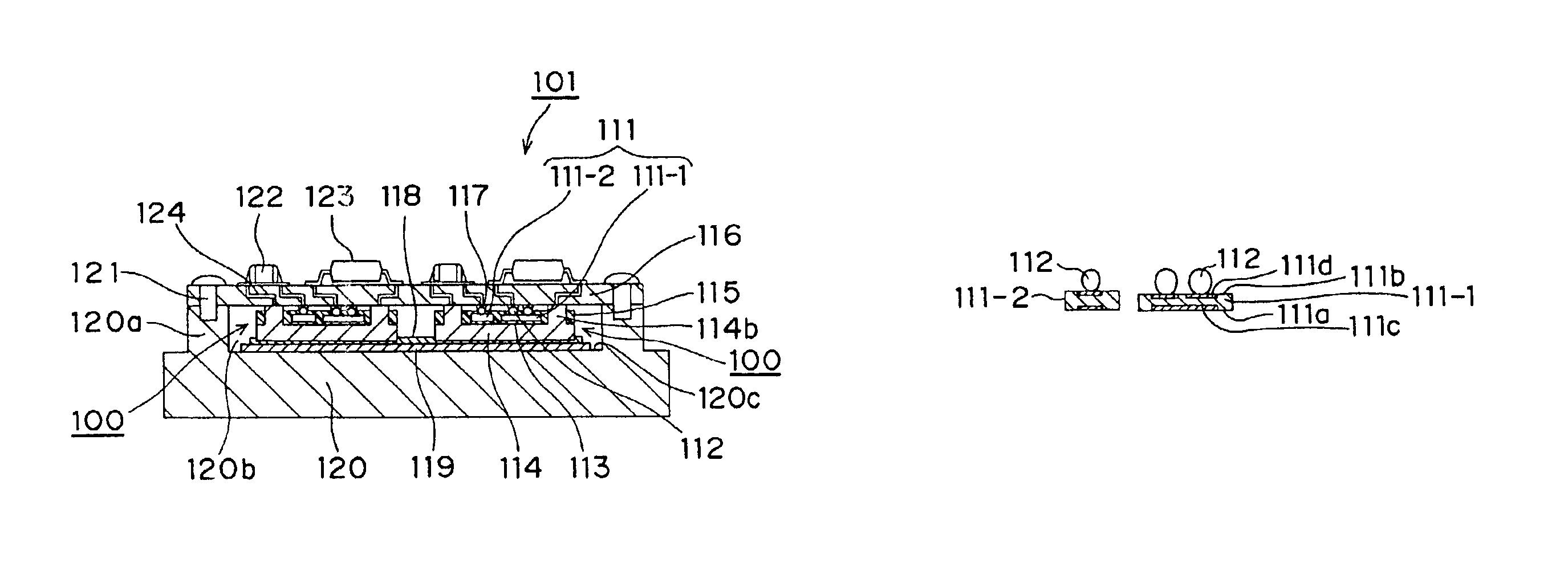
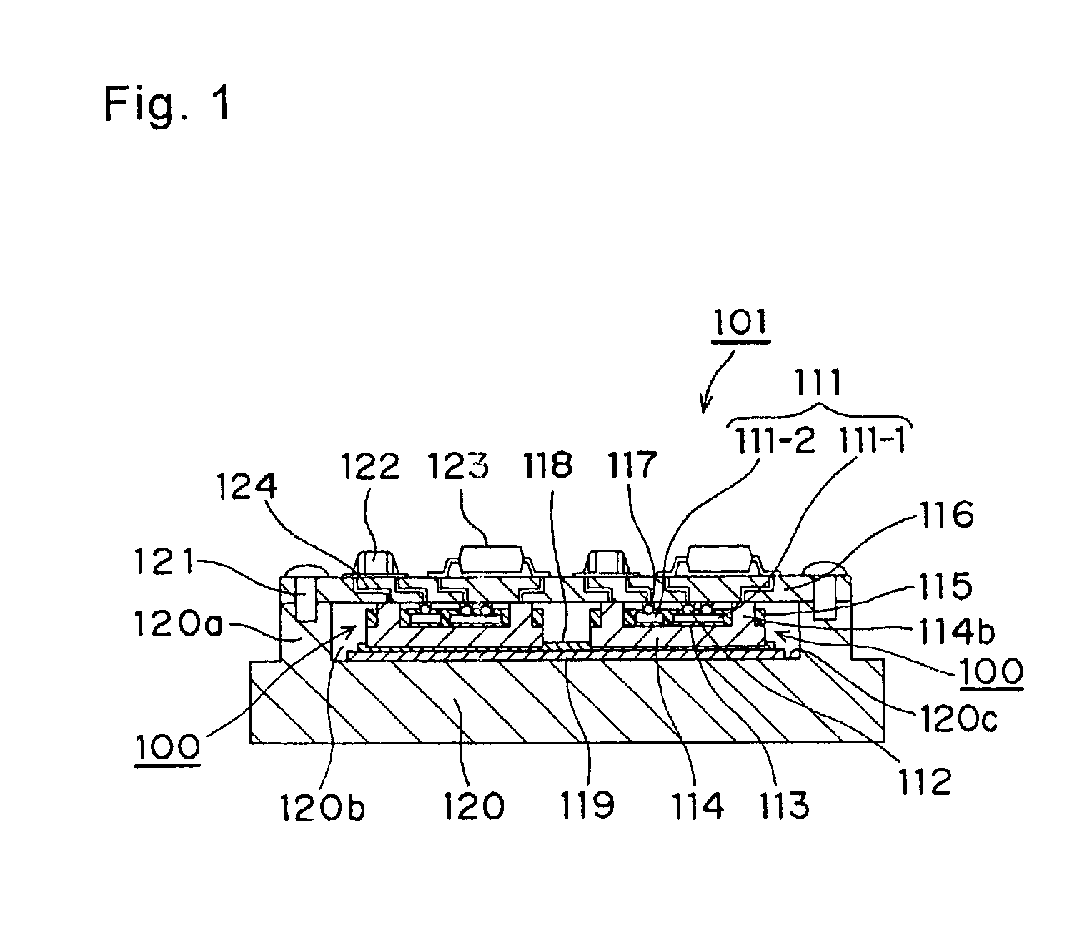
[0069]FIG. 5 shows a first electronic circuit device of a power control system (referred to as “a first circuit unit” hereinbelow) 100 which is one example of an electronic circuit device of this embodiment. FIG. 1 shows a second electronic device of a power control system (referred to as “a second circuit device” below) 101 including first circuit units 100, which corresponds to another example of an electronic circuit device.

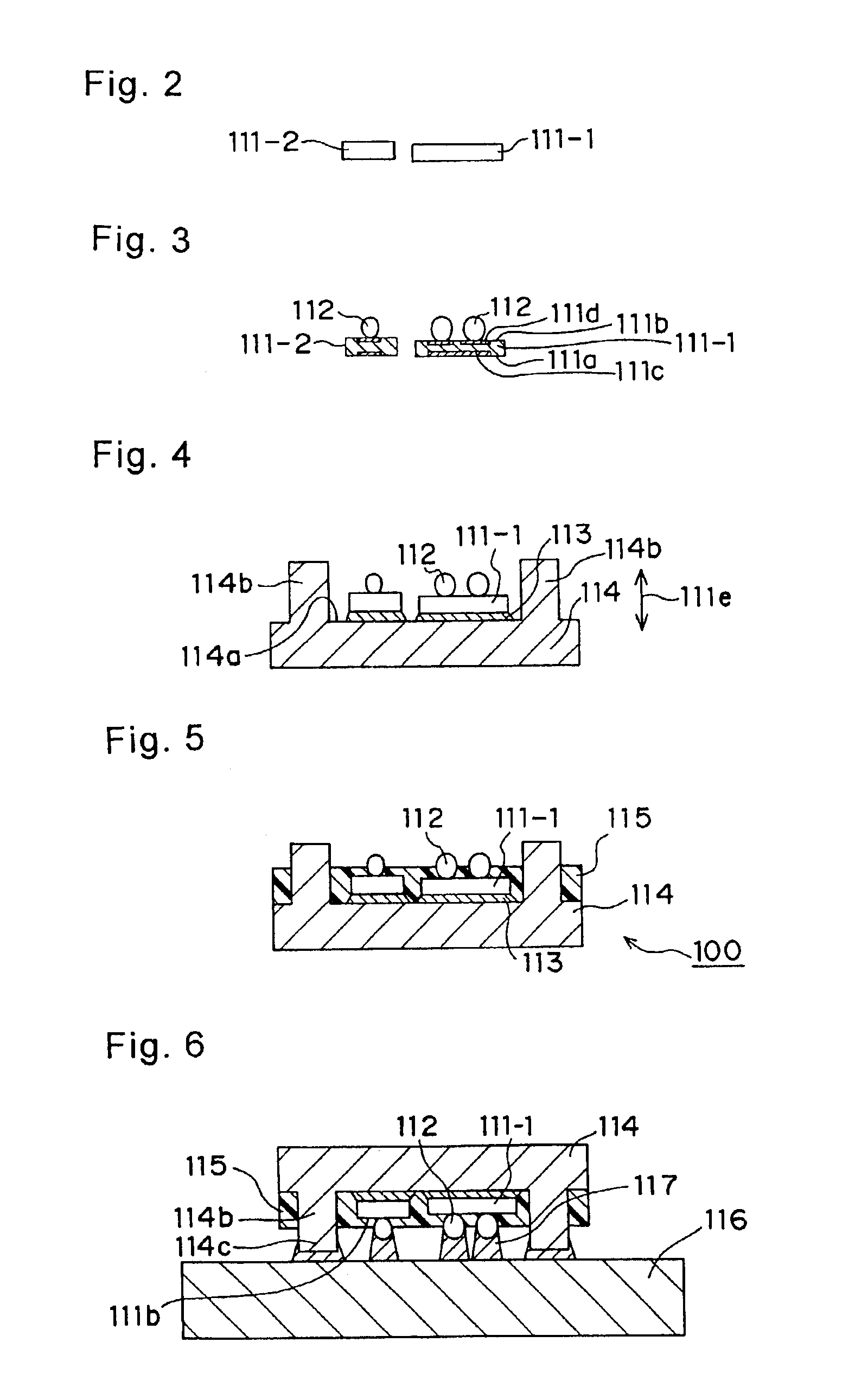
[0070]The second circuit device 101 of FIG. 1 is constituted as follows. 111 is a drive semiconductor element which is used in a control system for controlling a driving current to a driving device, e.g., a motor or the like and which requires a heat radiation treatment. The drive semiconductor element includes an IGBT (Insulated Gate Bipolar Transistor) 111-1 and a diode 111-2. As shown in FIG. 3, the drive semiconductor element 111 has a first electrode 111c and second electrodes 111d formed on opposite faces 111a and 111b, respectively. 112 are bumps (proje...

second embodiment

[0086]A fourth circuit device 103 as a modified example of the second circuit device 101 will be described with reference to FIG. 8.

[0087]The fourth circuit device 103 includes a third circuit unit 102 which is a modified example of the above first circuit unit 100. Reference numeral 133 of FIG. 8 indicates a first circuit board formed of a metal. Single-sided surface mounting is performed for the second circuit board 116 in FIG. 8.

[0088]The third circuit unit 102 has spring wires 136 of a metal and a second metallic member 134 respectively attached in place of the bumps 112 and the metallic member 114 of the first circuit unit 100. Each spring wire 136 is a conductor for electrically connecting the drive semiconductor element 111 and the second circuit board 116 to each other, and has a second bend portion 136a as indicated in FIG. 8. In the fourth circuit device 103 of FIG. 8, one end of each spring wire 136 penetrating the second circuit board 116 is soldered to the second circui...

third embodiment

[0095]A fifth circuit device 104 as a modified example of the second circuit device 101 will be depicted with reference to FIG. 10.

[0096]The fifth circuit device 104 has a constitution such that the projecting connector 22 and the dented connector 23 are removed from the driving device described with reference to FIG. 16, and a fresh metallic lead 139 is connected to metallic wire 18. Operation of removing bubbles described above is performed during soldering to join drive semiconductor element 111 and second metallic member 134 to one another. Single-sided surface mounting is provided for the second circuit board 116 in FIG. 8.

[0097]The metallic lead 139 is a metal wire having tin plating on copper, which is joined to aluminum metallic wire 18 subjected to wedge bonding of aluminum. A first bend portion 139a is formed in a halfway portion of the metallic lead 139. One end of the metallic lead 139 is soldered after passing through the second circuit board 116. Double-sided mounting ...


PUM

PropertyMeasurementUnit
temperatureaaaaaaaaaa
heights H1aaaaaaaaaa
metallicaaaaaaaaaa

Abstract

Bumps are formed on electrodes of semiconductor elements, and moreover, the semiconductor elements with the bumps are electrically connected to metallic members having installation members, whereby wiring lines are eliminated. Stray inductance and conduction resistance resulting from wiring lines can be reduced. A conventional dented connector and a projecting connector are eliminated by connecting the installation members to a second circuit board, thereby enabling an electronic circuit device of a power control system to be made compact.

Description

[0001]This application is a National Stage of PCT / JP02 / 00167 filed Jan. 15, 2002.TECHNICAL FIELD[0002]The present invention relates to an electronic circuit device of a power control system using semiconductor elements such as IGBTs (Insulated Gate Bipolar Transistors), diodes and the like, for driving motors, and a method for manufacturing the electronic circuit device.BACKGROUND ART[0003]Lately, a working current in a motor driving device has increased in accordance with an enhancement in performance and function of electronic devices used in the motor driving device, thereby requiring semiconductors to be used to meet a high current. A motor driving device used conventionally is shown in FIG. 16. An example of this conventional motor driving device will be described below with reference to FIG. 16.[0004]In FIG. 16, reference numerals respectively indicate: 1a an IGBT; 1b a diode; 3 a high temperature solder; 4 a metallic element; 5 a sealing resin; 6 a solder; 7 a circuit board; ...

Claims


Application Information

Patent Timeline
Patent Type & Authority Patents(United States)
IPC IPC(8): H01L23/58H01L23/64H01L25/16H05K1/14H01L25/07H01L21/60H01L23/49H01L23/492H01L23/495H01L25/18H01R13/648
CPCH01L23/492H01L23/49562H01L23/645H01L24/33H01L24/83H01L25/072H01L25/162H01L24/81H01L2224/13144H01L2224/16H01L2224/291H01L2224/48091H01L2224/48137H01L2224/48247H01L2224/48472H01L2224/73153H01L2224/73253H01L2224/81193H01L2224/81801H01L2224/8319H01L2224/83801H01L2924/01004H01L2924/01013H01L2924/01029H01L2924/01033H01L2924/0105H01L2924/01057H01L2924/01078H01L2924/01079H01L2924/01082H01L2924/13055H01L2924/15153H01L2924/15165H01L2924/15174H01L2924/16152H01L2924/16195H01L2924/19041H01L2924/19043H01L2924/30107H05K1/144H01L24/48H01L2924/01006H01L2924/014H01L2224/45124H01L2224/45144H01L2224/45147H01L2224/16225H01L2224/32245H01L2224/73265H01L2924/1305H01L2924/00014H01L2924/00H01L2924/351H01L2224/85205H01L2924/00011H01L24/45H01L2224/05571H01L2224/05573H01L2224/48139H01L2924/181H01L2924/00015H01L2224/83205H01L2924/00012
Inventor NOBORI, KAZUHIROIKEDA, SATOSHIKATO, YASUSHINAKAJIMA, YASUFUMI
Owner PANASONIC CORP
Why Eureka
Try Eureka