Device and method for controlling focussed electron beams

a technology of focused electron beams and devices, which is applied in the direction of static indicating devices, discharge tubes luminescnet screens, instruments, etc., can solve the problems of beam current stability, beam current instabilities, and high operational vacuum, and achieve compact and rigid setup, cost-effective, and high precision.

Inactive Publication Date: 2005-09-13
ICT INTEGRATED CIRCUIT TESTING GESELLSCHAFT FUER HALBLEITERPRUEFTECHNIK GMBH
View PDF14 Cites 17 Cited by
  • Summary
  • Abstract
  • Description
  • Claims
  • Application Information

AI Technical Summary

Benefits of technology

[0018]Therefore, in a first aspect of the present invention a focussing electron beam device is provided with an electron beam whose actual current value is sensed for deviations from a desired current value and adjusted to a desired current value without sacrificing control of the focus position of the electron beam. In a second aspect of the present invention a focussing electron beam device is provided with an array of electron beams where the actual beam current values of the electron beams can be adjusted to desired current values without sacrificing control of the focus positions. This allows the compensation of focus position shifts of the electron beam caused by changes of the first voltage V1 to stabilize the electron beam current value. Sensing for the deviations of the actual current value from the desired current value, adjusting the first voltage V1 and adjusting the second voltage V2 are preferably automatically performed by the control circuit.
[0054]Preferably active electronic components, e.g. transistors or diodes, of the control circuit are integrated onto the substrate. Using thin film techniques it is possible to integrate active electronic components of the control circuit onto the substrate in order to minimize the space and to be able to bias the possibly thousands of field emitter beam sources. Furthermore, the integration of the electronic components close to the field emitter beam sources minimizes electromagnetic interference and malfunction due to cable defects and the like. In particular, the high integration density allows for a complex control circuitry at little space which is necessary to adjust the first or second voltages, V1 or V2, for each field emitter beam source individually.

Problems solved by technology

The price to be paid for these advantages are a high operational vacuum (−9 mbar) and, related to this, problems with the beam current stability.
The beam current instabilities, however, represent a limitation to imaging resolution or to the homogeneity for structuring the surface of specimens.
However, the problem then arises that the electrical potential of the extraction electrode fluctuates, which can deteriorate the focus stability of the electron beam.
However, the problem of fluctuating beam currents of field emitter beam sources is even more severe when an array of beams is used.
Such artifacts would limit the resolution of the image or of the structure on the surface of the specimen.

Method used


Image

  • Device and method for controlling focussed electron beams
  • Device and method for controlling focussed electron beams
  • Device and method for controlling focussed electron beams

Examples


Embodiment Construction

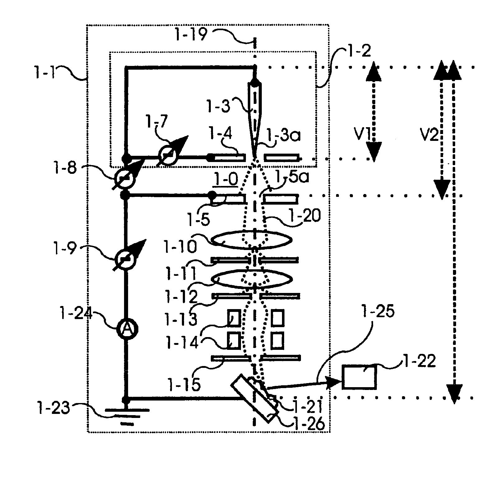
[0069]A focussing electron beam device of the prior art is shown schematically in FIG. 1 and has been described in detail in the chapter describing the background of the invention.

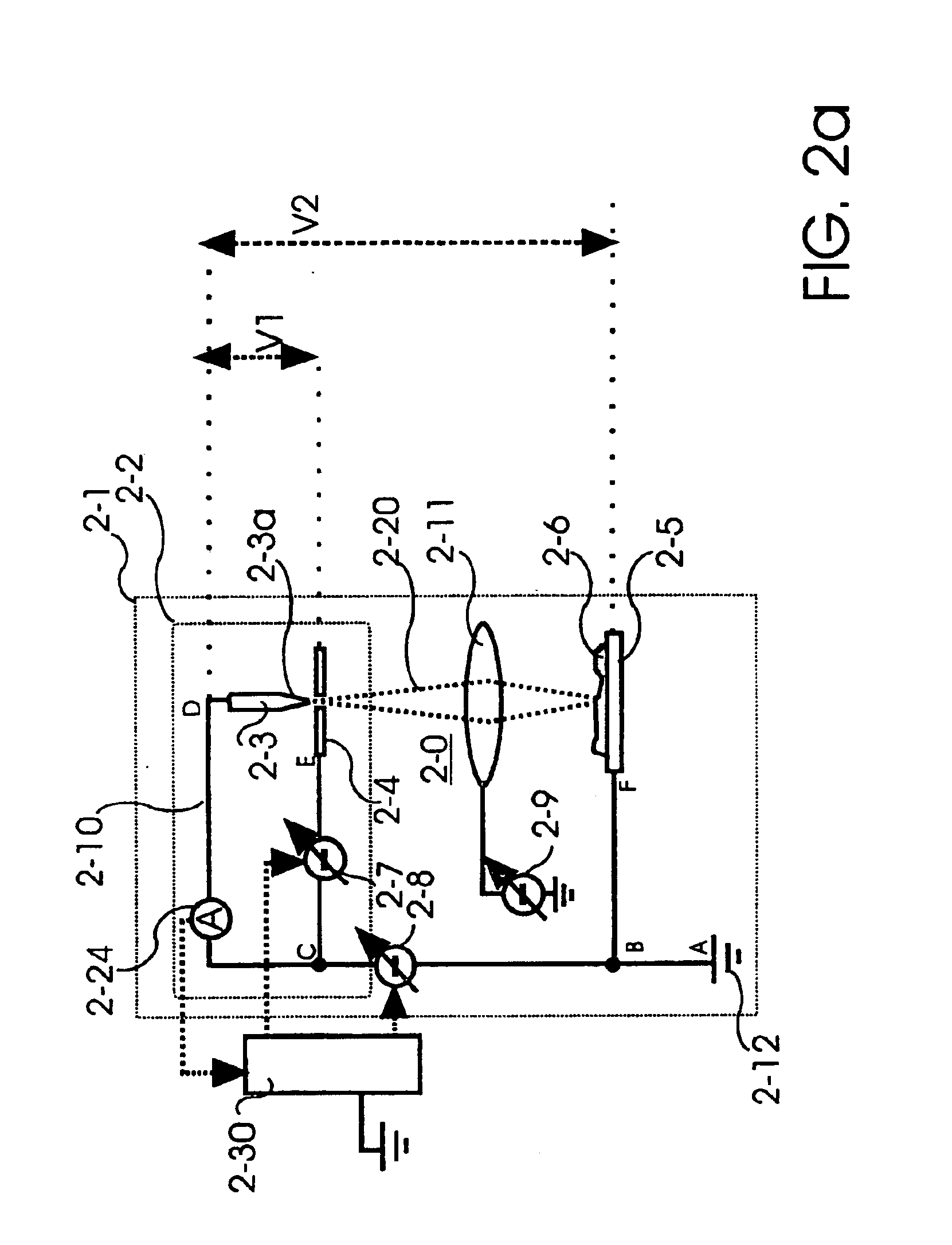
[0070]FIG. 2a describes schematically an electron beam column 2-1 of a first embodiment according to the invention. The focussing electron beam device 2-1 comprises a field emitter beam source 2—2, focussing components 2-11, a specimen 2-6 on an anode 2-5. The field emitter beam source 2—2 comprises an emitter 2-3 with an emitter tip 2-3a, an extraction electrode 24 and a 1st voltage source 2-7 applying its voltage between the emitter 2-3 and the extraction electrode 24 on a cable tree 2-10. The word “cable tree” has to be understood in a broad sense, i.e. it can comprise cables, conducting leads on a printed circuit board, conducting leads on a semiconductor substrate or other leads to make electrical connections. In this embodiment of the invention, the 1st voltage source is applied between the nodes E a...


PUM


Abstract

The invention provides a focussing electron beam device with a single or an array of field emitter beam sources to generate electron beams with field emitter beam sources, at least one anode capable of accelerating the electrons of the electron beams towards a specimen, focussing components capable of focussing the electron beams onto the specimen and a control circuit that a) senses for deviations of the actual current values of the electron beams from desired current values; b) controls first voltages V1 to adjust the actual current values of the electron beams to the desired current values and c) controls second voltages V2 to adjust the actual focus positions of the electron beams to the desired focus positions. The voltage control circuit adjusts the actual current values of the electron beams to the desired current values and makes it possible to adjust the current values of an array of electron beams to a single value. Furthermore, a focussing electron beam device is disclosed with an array of field emitter beam sources integrated onto a substrate, which makes it possible to have arrays of field emitter beam sources with thousands or even millions of field emitter beam sources. With the integration of the control circuits for each field emitter beam source it is possible to adjust the current values and focus positions of each electron beam individually. Furthermore, methods are disclosed describing the operation of a single field emitter beam source or an array of field emitter beam sources.

Description

FIELD OF THE INVENTION[0001]The invention relates to a focussing electron beam device and to a method to control focussed electron beams. In particular, this invention relates to a focussing electron beam device with focussed electron beams to examine a specimen or to structure the surface of a specimen.BACKGROUND OF THE INVENTION[0002]Focussed electron beam devices, like e.g. electron microscopes for inspecting specimen or electron beam pattern generators for structuring surfaces of a specimen use electron beams because of their spatial resolution, which can be several orders of magnitude higher than the one of optical light beam devices.[0003]A central part of a focussing electron beam device is the electron beam column which generates the electron beam, accelerates the electrons of the beam to a desired energy and focusses the beam. The electron beam is generated by some kind of electron beam source, accelerated by a voltage between the electron beam source and one or several ano...

Claims


Application Information

Patent Timeline
Patent Type & Authority Patents(United States)
IPC IPC(8): H01J37/30H01J37/304H01J37/06H01J37/073
CPCH01J37/073H01J37/304H01J2237/06316H01J2237/0635H01J2237/31774
Inventor WINKLER, DIETERADAMEC, PAVEL
Owner ICT INTEGRATED CIRCUIT TESTING GESELLSCHAFT FUER HALBLEITERPRUEFTECHNIK GMBH
Why Eureka
Try Eureka