Method for manufacturing semiconductor device having porous structure with air-gaps

a technology of porous structure and air gap, which is applied in the direction of semiconductor devices, semiconductor/solid-state device details, electrical devices, etc., can solve the problems of difficult to achieve the effect of achieving the effect of achieving good mechanical properties, excellent applicability to the dual damascene process, and excellent mechanical properties

Active Publication Date: 2005-09-27
ASM JAPAN
View PDF12 Cites 88 Cited by
  • Summary
  • Abstract
  • Description
  • Claims
  • Application Information

AI Technical Summary

Benefits of technology

[0010]In an aspect, an embodiment of the present invention provides a method for manufacturing a semiconductor device, comprising the steps of: (i) depositing a sacrificial layer on a substrate having a circuit formed thereon; (ii) etching the sacrificial layer except for a portion where air gaps are to be formed; (iii) depositing a low-dielectric layer over the substrate until the portion for air gaps is entirely enclosed in the low-dielectric layer; (iv) etching the low-dielectric layer to form via holes (“vias”) and trenches therethrough; (v) prior or subsequent to step (iv), removing the portion for air gaps of the sacrificial layer; and (vi) depositing copper in the vias and trenches which are filled with the copper contacting a surface of the substrate. By the above method, an ELK film having excellent mechanical properties and excellent applicability to the Dual Damascene process can effectively and easily be obtained. In the above, an etch stop layer can be used before depositing a low-k film. The purpose of the etch stop layer may have two folds; as a mechanical support and as a reference etch stop layer for stopping etch.

Problems solved by technology

However, this approach has disadvantages: The deposited dielectric layer has a very high porosity (e.g., >30%) with bimodal or trimodal pores with pore sizes ranging from 2 nm to 9 nm or higher.
Thus, mechanical properties of the layer are very low, particularly hardness and cohesive strength.
Also, because of large pores, new and costly processes may be required for the Dual Damascene integration with copper.
This processes may result in poor yields and also pose very high challenge for successful integration with copper.

Method used


Image

  • Method for manufacturing semiconductor device having porous structure with air-gaps
  • Method for manufacturing semiconductor device having porous structure with air-gaps
  • Method for manufacturing semiconductor device having porous structure with air-gaps

Examples


Embodiment Construction

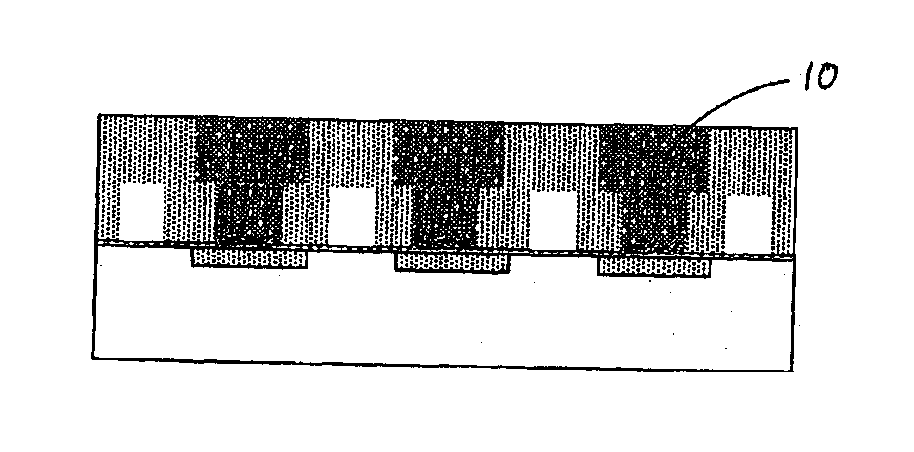
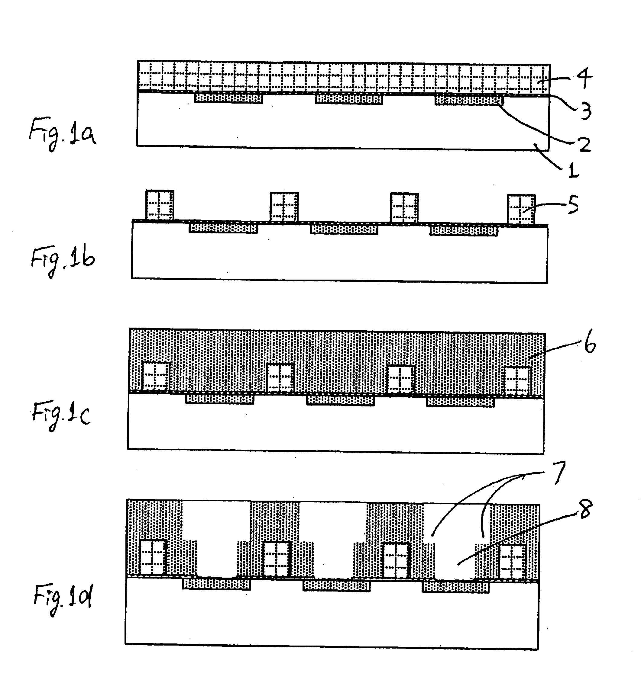
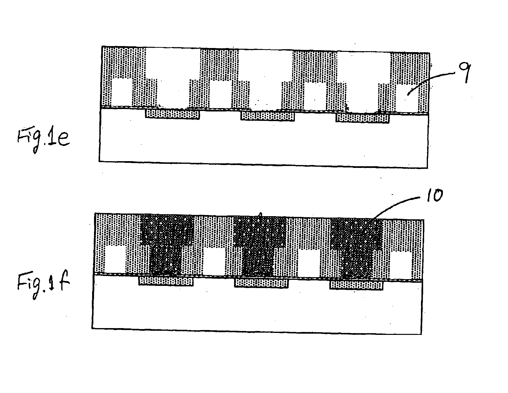
[0027]As described above, in an aspect, the present invention provides a method for manufacturing a semiconductor device, which method can be performed using any suitable plasma CVD chambers which can be operated as one operation system. This is an advantage of the present invention. However, chambers specifically designed for respective steps can be used. The method is suitable for any Damascene process, especially the Dual Damascene process which is described in U.S. Pat. No. 6,440,838 or U.S. Pat. No. 6,440,861, for example, the disclosure of which is incorporated herein by reference in its entirety.

[0028]An embodiment comprises the steps of: (i) depositing a sacrificial layer on a substrate having a circuit formed thereon; (ii) etching the sacrificial layer except for a portion where air gaps are to be formed; (Add the comment written above for etch stop layer option) (iii) depositing a low-dielectric layer over the substrate until the portion for air gaps is entirely enclosed i...


PUM


Abstract

A method for manufacturing a semiconductor device includes: (i) depositing a sacrificial layer made of an organic polymer such as benzocyclobutene on a substrate having a circuit formed thereon; (ii) etching the sacrificial layer except for a portion where air gaps are to be formed; (iii) depositing a low-dielectric layer over the substrate until the portion for air gaps is entirely enclosed in the low-dielectric layer; (iv) etching the low-dielectric layer to form via holes and trenches there through; (v) prior or subsequent to step (iv), removing the portion for air gaps; and (vi) depositing copper in the vias and trenches which are filled with the copper contacting a surface of the substrate.

Description

[0001]This Application Non-Provisional of 60 / 422,956 Oct. 31, 2002 Pending.BACKGROUND OF THE INVENTION[0002]1. Field of the Invention[0003]This invention relates to methods of manufacturing semiconductor devices having a porous structure and voids (air-gaps), and particularly relates to methods that involve selectively etching a sacrificial film.[0004]2. Description of the Related Art[0005]In recent years, semiconductor devices have become faster and more highly integrated and resistance-capacitance (RC) coupling delays have become a large factor in signal processing time. RC delays can be decreased by reducing wiring capacitance. One way to do this is to use low dielectric constant materials such as fluorine-doped SiO2, porous SiO2, an organic film or a porous film, etc. However, these materials have not been put to practical use because of problems such as processing difficulty and insufficient heat-resistance, which can increase the complexity of the integration processes and low...

Claims


Application Information

Patent Timeline
Patent Type & Authority Patents(United States)
IPC IPC(8): H01L21/70H01L21/768H01L23/522
CPCH01L21/76807H01L21/7682H01L21/76835
Inventor KUMAR, DEVENDRA
Owner ASM JAPAN
Why Eureka
Try Eureka