Interferometric modulation pixels and manufacturing method thereof

a technology of interferometry and modulation pixel, which is applied in the field of planar panel display, can solve the problems of damage to the surface adverse effects on the optical thin film of the bottom electrode, and damage to the /b>, so as to enhance the image display quality of the planar optical interference display and stabilize the quality of the optical thin film

Active Publication Date: 2005-10-04
SNAPTRACK
View PDF3 Cites 221 Cited by
  • Summary
  • Abstract
  • Description
  • Claims
  • Application Information

AI Technical Summary

Benefits of technology

[0012]In one aspect, the present invention provides an interferometric modulation pixel and a manufacturing method of which a protection layer is formed on the bottom electrode to protect the upper surface of the bottom electrode.
[0013]In another aspect, the present invention provides an interferometric modulation pixel and a manufacturing method of which a protection layer is formed on the bottom electrode to stabilize the quality of the optical thin film of the bottom electrode.
[0014]In yet another aspect, the present invention provides an interferometric modulation pixel and a manufacturing method that enhances the image display quality of the planar optical interference display.
[0018]In light of the preferred embodiments of the present invention described above, a non-silicon protection layer covers the insulating layer of the bottom electrode to separate the sacrificial layer from the insulating layer, both of which are silicon-based. Hence, the bottom electrode surface is not damaged by the etchant, and the bottom electrode structure is thereby kept intact to provide high display quality for an optical interference display.

Problems solved by technology

However, if the etchant that is used to remove the sacrificial layer does not properly etch selectively, the surface of the bottom electrode 102 is damaged such that the cavity depth D and the optical thin film of the bottom electrode are adversely affected.
That is, the reflected wavelength λ1 is different from what is intended, damaging the color uniformity of the optical interference display.

Method used


Image

  • Interferometric modulation pixels and manufacturing method thereof
  • Interferometric modulation pixels and manufacturing method thereof
  • Interferometric modulation pixels and manufacturing method thereof

Examples


Embodiment Construction

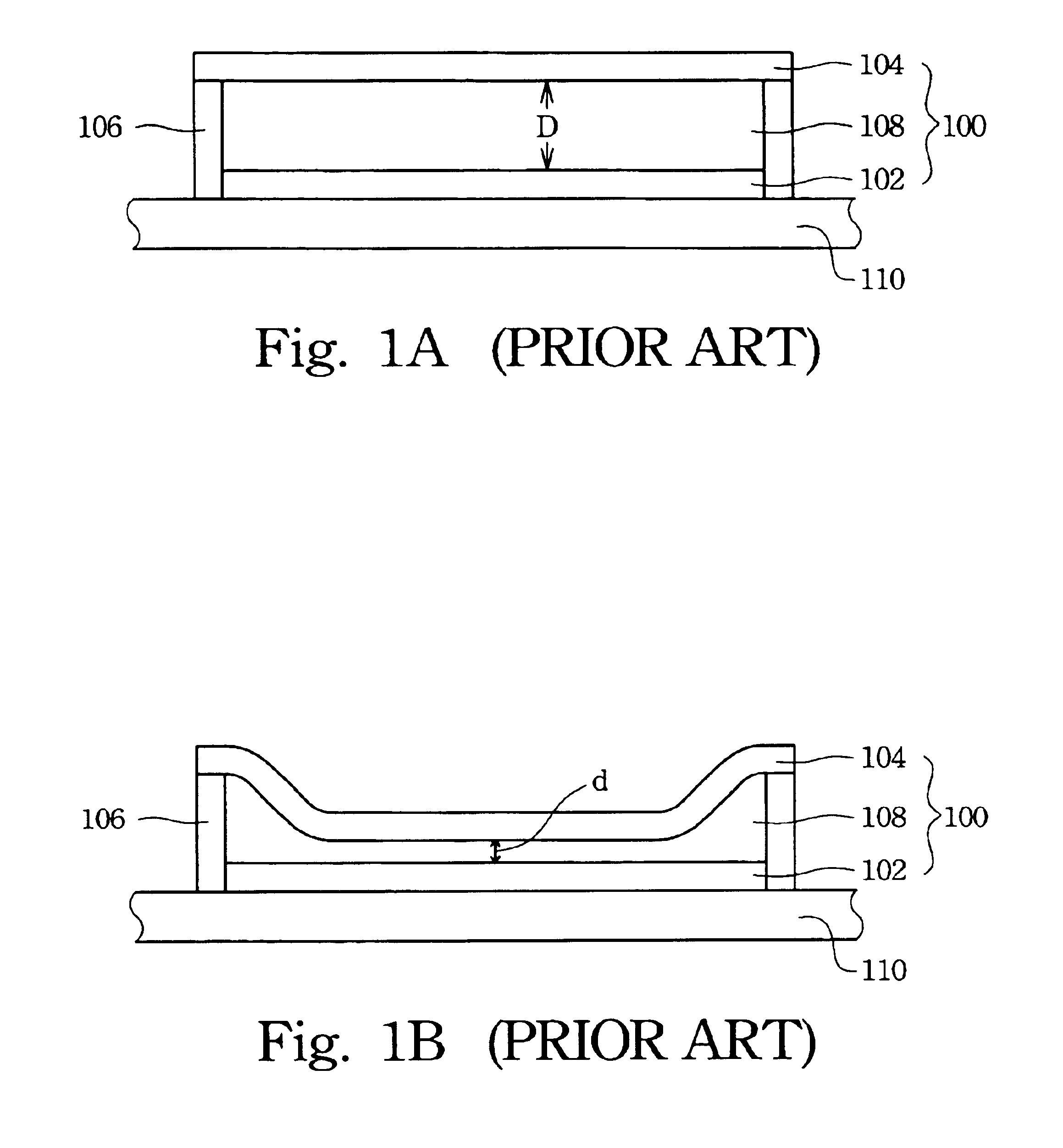
[0024]This invention provides an interferometric modulation pixel and a manufacturing method thereof that eliminates damage on the bottom electrode surface occurring during the sacrificial layer removal process. In a preferred embodiment of this invention, the bottom electrode is covered by a protection layer. Therefore, the bottom electrode surface is not damaged by the etchant used to remove the sacrificial layer, and the bottom electrode structure is kept intact so as to provide high display quality for the optical interference display.

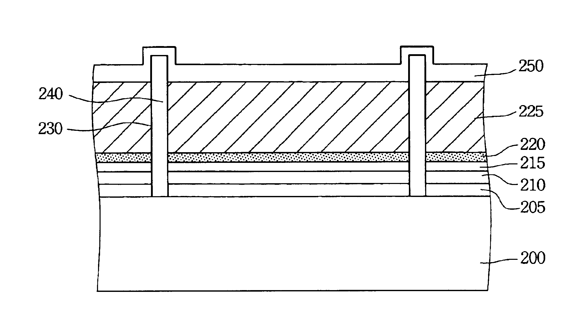
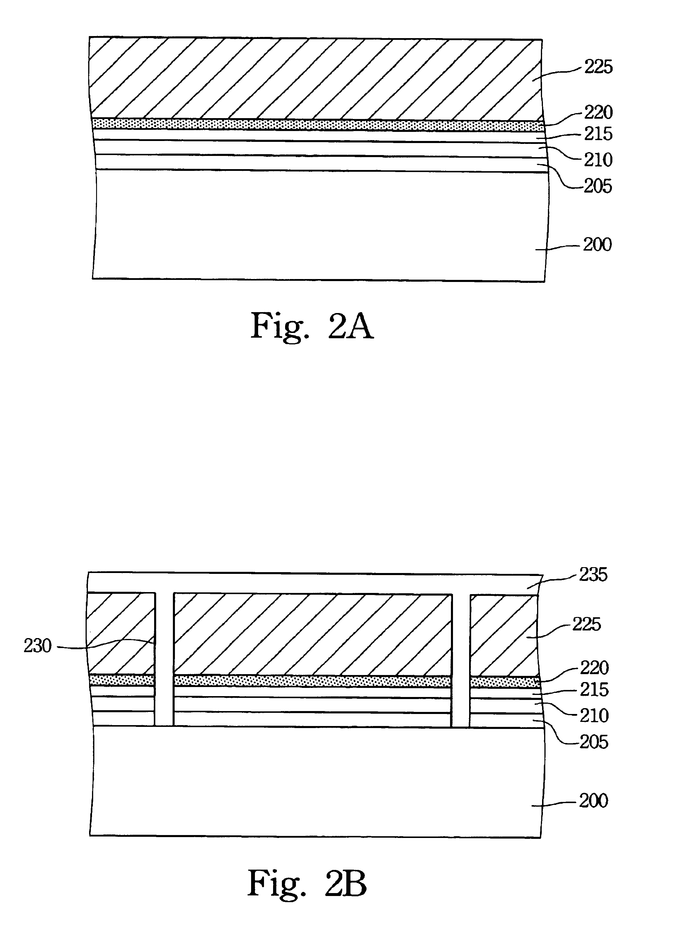
[0025]Reference will now be made in detail to the present preferred embodiments of the invention, examples of which are illustrated in the accompanying drawings. FIGS. 2A-2D are cross-sectional diagrams showing a process of manufacturing an interferometric modulation pixel according to a preferred embodiment of this invention.

[0026]In FIG. 2A, a transparent conductive layer 205, a light-absorption layer 210, an insulating layer 215, a protection la...


PUM

PropertyMeasurementUnit
depthaaaaaaaaaa
transparentaaaaaaaaaa
photosensitiveaaaaaaaaaa

Abstract

A protection layer covers the cavity-side surface of a bottom electrode of a interferometric modulation pixel. Consequently, the protective layer protects the surface of the bottom electrode while a sacrificial layer between the bottom electrode and the top electrode is being etched. Thus, the distance between the bottom electrode and the top electrode is maintained, thereby ensuring that only the light with desired wavelengths is reflected by the interferometric modulation pixel.

Description

BACKGROUND[0001]1. Field of Invention[0002]The present invention relates to a planar panel display and a manufacturing method thereof. More particularly, the present invention relates to an interferometric modulation pixel and a manufacturing method thereof.[0003]2. Description of Related Art[0004]Planar displays are extremely popular in the portable and limited-space display market because they are lightweight and small. To date, in addition to liquid crystal display (LCD), organic light-emitting diode (OLED) and plasma display panel (PDP) display panels, a module of the optical interference display has been investigated.[0005]The features of an interferometric modulation pixel of the optical interference display include low electrical power consumption, short response time and bi-stable status. Therefore, the optical interference display can be applied in planar display panels, especially in portable products such as mobile phones, personal digital assistants (PDA), and portable c...

Claims


Application Information

Patent Timeline
Patent Type & Authority Patents(United States)
IPC IPC(8): G02B26/00G02F1/1335G02F1/13G02F1/21
CPCG02B26/001G02B26/00
Inventor LIN, WEN-JIANTSAI, HSIUNG-KUANG
Owner SNAPTRACK
Why Eureka
Try Eureka