Controlled selectivity etch for use with optical component fabrication

a technology of selective etching and optical components, which is applied in the direction of photomechanical equipment, instruments, photosensitive material processing, etc., can solve the problems of inconvenient forming of etches and limited etching to vertical surfaces of optical components

Inactive Publication Date: 2006-02-28
KOTURA
View PDF45 Cites 18 Cited by
  • Summary
  • Abstract
  • Description
  • Claims
  • Application Information

AI Technical Summary

Benefits of technology

[0009]In some instances, the upper surface of the mask is smoother than the upper surface of the underlying medium. The etch can substantially transfer the upper surface of the mask to the upper surface of the underlying medium and can accordingly smooth the upper surface of the underlying medium.

Problems solved by technology

Because the mask remains intact during these etches, the etches are limited to forming vertical surfaces of the optical component.
Accordingly, these etches are not suitable for forming complex features such as vertical tapers on an optical component.

Method used


Image

  • Controlled selectivity etch for use with optical component fabrication
  • Controlled selectivity etch for use with optical component fabrication
  • Controlled selectivity etch for use with optical component fabrication

Examples


example 1

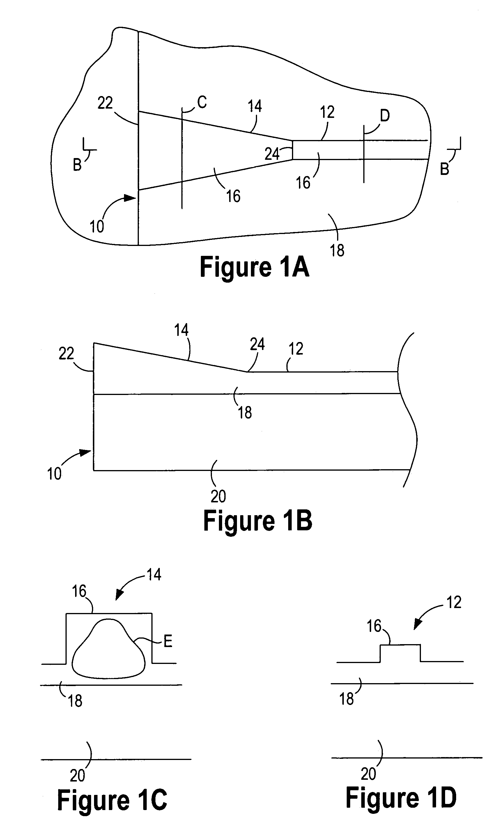
[0097]The following example is performed on a Decoupled Plasma Source Deep Trench etcher (DPSDT) manufactured by Applied Materials. An optical component precursor is positioned in the chamber. The optical component includes silicon as the light transmitting medium. One or more portions of the optical component are masked with a photoresist having a region with a vertical taper. The optical component precursor is etched by delivering an etching medium having SF6 as the first etchant and CF4 as the second etchant. The SF6 flow rate is about 6 sccm and the CF4 flow rate is about 60 seem so as to maintain the chamber pressure at about 4 mTorr. The source power is operated at 700 W and 13.56 MHz. The cathode is operated at 120 W and 400 KHz and at a temperature of about 10° C. The etch is performed for a period of time needed to etch through at least the portion of the mask having the taper. Accordingly, at least a portion of the vertical taper is transferred to the optical component pre...

example 2

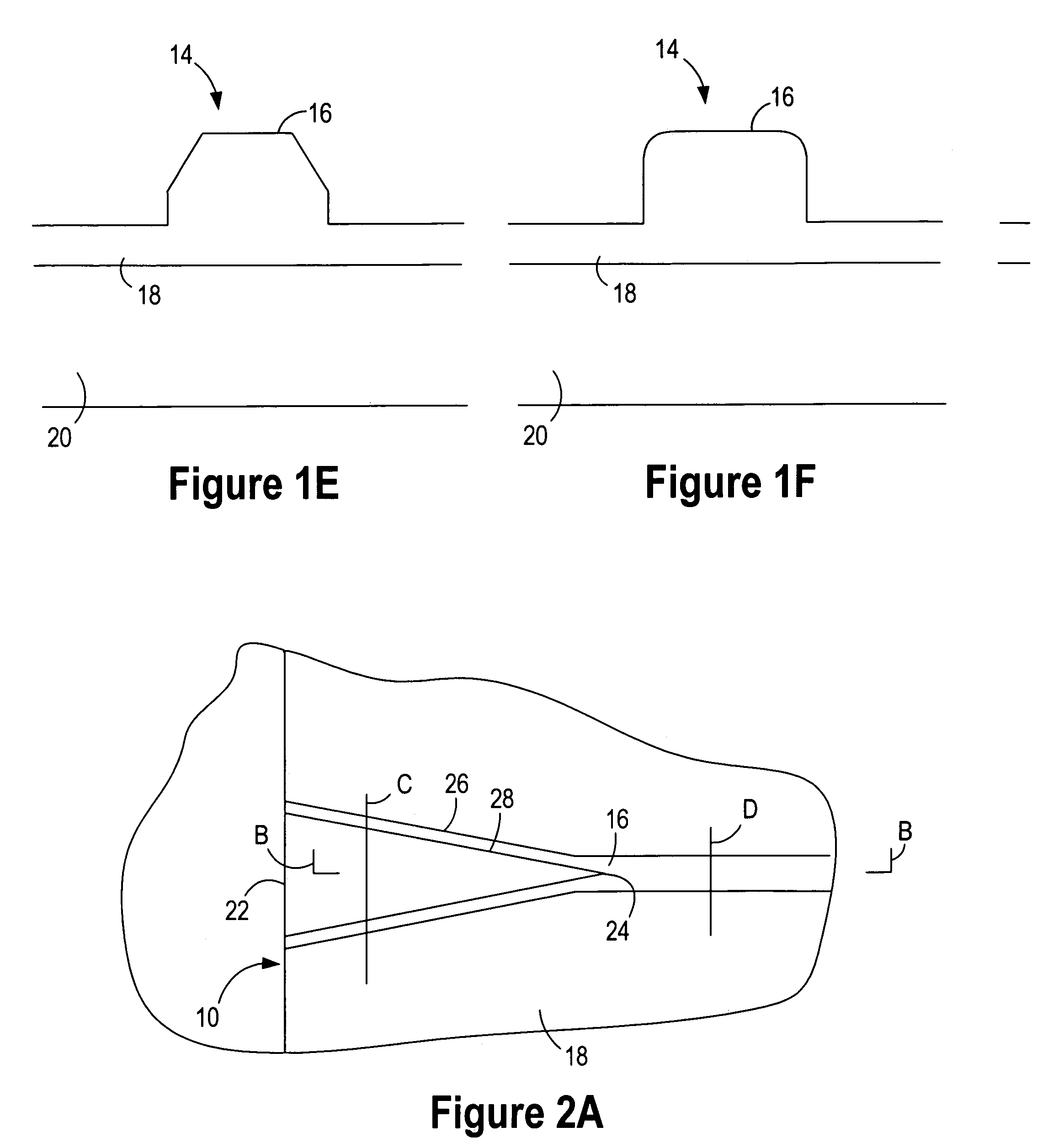
[0098]The following example is performed on a Decoupled Plasma Source Deep Trench etcher (DPSDT) manufactured by Applied Materials. An optical component precursor is positioned in the chamber. The optical component includes single crystal Si in some area and poly Si in other areas as the light transmitting medium. The surface of poly Si is rough and the interface of single crystal Si and poly Si have a roughness on the order of 1 um. A photoresist is spin coated on the surface having the smoothness of about 10 nm. The optical component precursor is etched by delivering an etching medium having SF6 as the first etchant and CF4 as the second etchant. The SF6 flow rate is about 6 sccm and the CF4 flow rate is about 60 sccm so as to maintain the chamber pressure at about 4 mTorr. The Source RF power is operated at 700 W and 13.56 MHz. The cathode is operated at 120 W and 400 KHz and at a temperature of about 110° C. The etch is performed for a period of time needed to etch through the r...

example 3

[0099]The following example is performed on a Decoupled Plasma Source Deep Trench etcher (DPSDT) manufactured by Applied Materials. An optical component precursor is positioned in the chamber. An alternative gas combination and ratio can be used to etch waveguide with the selectivity of Si to resist as desired ratio. The optical component includes silicon as the light transmitting medium. The optical component precursor is etched by delivering an etching medium having SF6 as the first etchant and CF4 as the second etchant. The SF6 flow rate is about 20 sccm and the CHF3 flow rate is about 60 sccm so as to maintain the chamber pressure at about 4 mTorr. The Source RF power is operated at 1000 W and 13.56 MHz. The cathode is operated at 30 W and 400 KHz and at a temperature of about 101C. The etch is performed for a period of time needed to etch to get the desired WG depth. The selectivity of Si to resist is 2:1.

[0100]The methods of FIG. 4A through FIG. 6O each employ one or more etch...


PUM

PropertyMeasurementUnit
RF DC bias poweraaaaaaaaaa
pressureaaaaaaaaaa
pressureaaaaaaaaaa

Abstract

A method of fabricating an optical component includes forming a mask on an optical component precursor. The method also includes etching through at least a portion of the mask so as to etch an underlying medium concurrently with remaining mask and transfer a feature of an upper surface of the mask onto an upper surface of the underlying medium. The etch can be configured such that a ratio of the underlying medium etch rate to the mask etch rate is less than about 1.5:1. In some instances, the underlying medium is silicon and the mask is a photoresist.

Description

RELATED APPLICATIONS[0001]This application is related to U.S. patent application Ser. No. 09 / 845,093, filed on Apr. 27, 2001, entitled “Formation of an Optical Component” and incorporated herein in its entirety, now abandoned. This application is also related to U.S. patent application Ser. No. 10 / 072,811, filed on Feb. 8, 2002, entitled “Formation of an Optical Component Having Smooth Sidewalls” and incorporated herein in its entirety, now abandoned.[0002]This application is a continuation-in-part of U.S. patent application Ser. No. 10 / 236,505, filed on Sep. 6, 2002, entitled “Optical Component Having Waveguides Extending from a Common Region” and incorporated herein in its entirety, allowed.BACKGROUND[0003]1. Field of the Invention[0004]The invention relates to fabrication of optical components. In particular, the invention relates to etches having controlled selectivity and related optical component applications.[0005]2. Background of the Invention[0006]Two-dimensional optical de...

Claims


Application Information

Patent Timeline
Patent Type & Authority Patents(United States)
IPC IPC(8): G03F7/26G02B6/12G02B6/138G02B6/34
CPCG02B6/12011G02B6/12016G02B6/138G02B2006/121G02B2006/12097
Inventor FONG, JOANQIAN, WEIZHENG, DAWEISHAO, ZHIANCHUNG, LIH-JOUYIN, XIAOMING
Owner KOTURA
Why Eureka
Try Eureka