Programming method of nonvolatile semiconductor memory device

a nonvolatile semiconductor and memory device technology, applied in static storage, digital storage, instruments, etc., can solve the problems of increasing the current peak at the programming time, especially the current consumption at the programming tim

Inactive Publication Date: 2005-10-11
SHARP KK
View PDF4 Cites 37 Cited by
  • Summary
  • Abstract
  • Description
  • Claims
  • Application Information

AI Technical Summary

Benefits of technology

[0024]Accordingly, the present invention has been achieved in view of the above-described problem and an object of the invention is to provide a method for programming multi-value data quickly into a nonvolatile semiconductor memory device capable of storing three-valued or higher valued data.

Problems solved by technology

Here, because if the threshold voltage before programming of the programming target memory cell is low and the threshold voltage after the programming is high, the applied program gate voltage is increased, an excessive drain current flows to the memory cell so that consumption current at the programming time, particularly its peak current increases.

Method used


Image

  • Programming method of nonvolatile semiconductor memory device
  • Programming method of nonvolatile semiconductor memory device
  • Programming method of nonvolatile semiconductor memory device

Examples


first embodiment

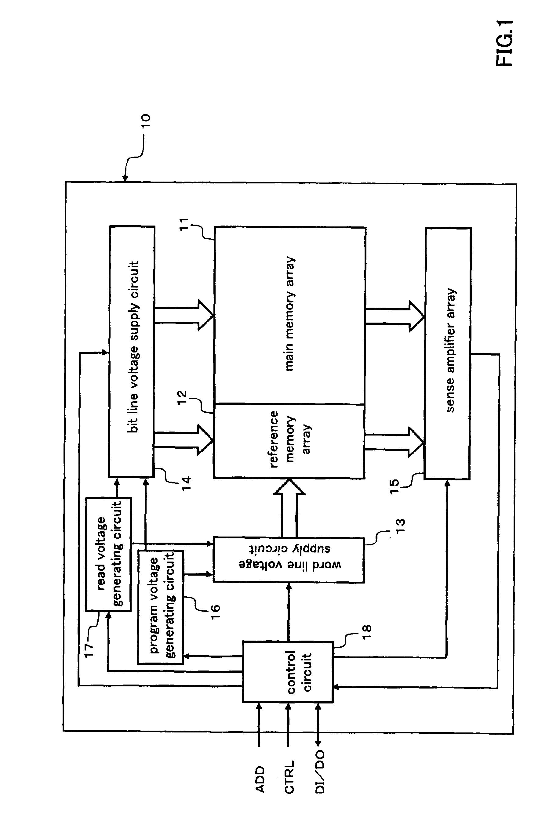
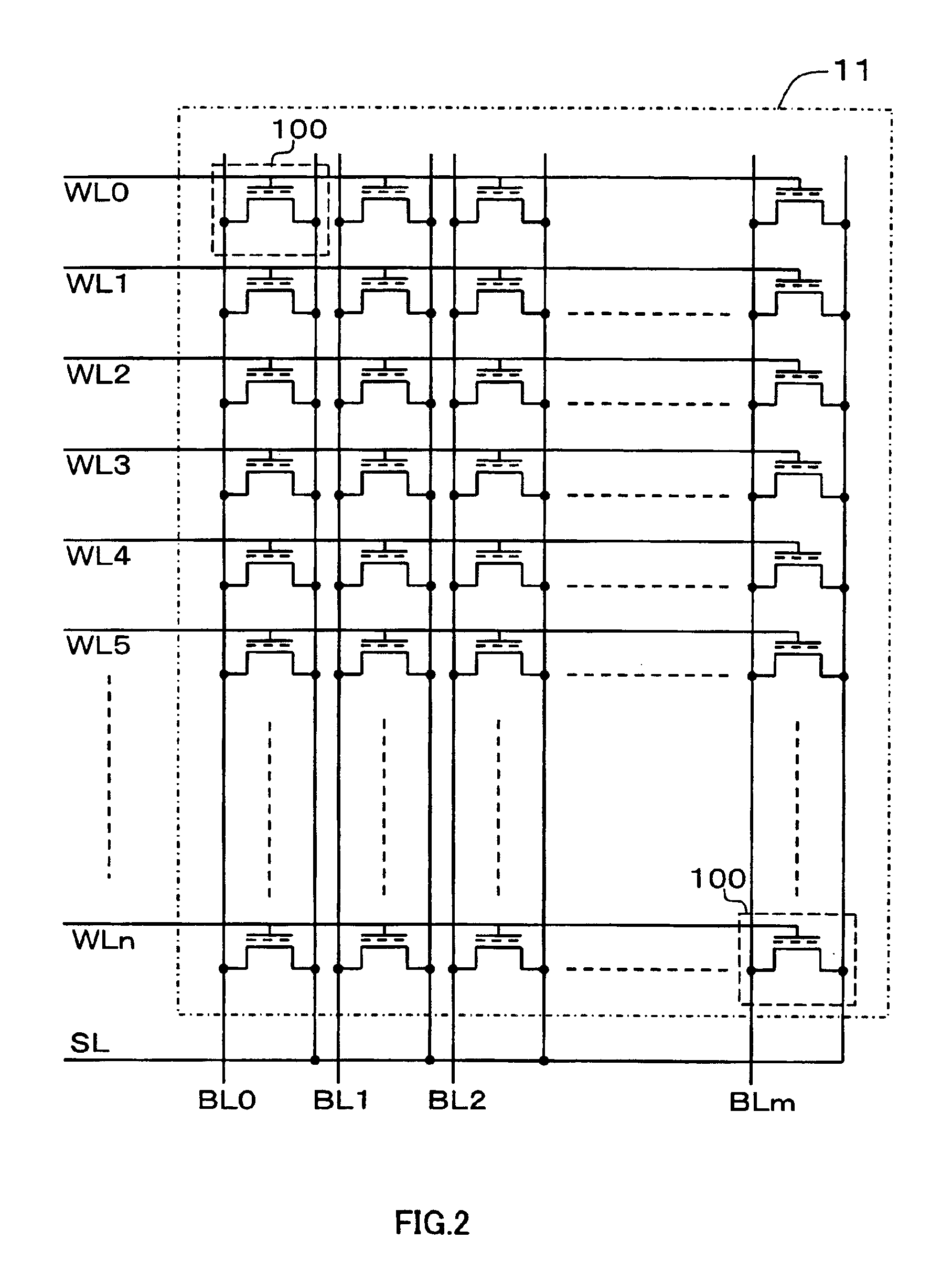
[0075]FIG. 1 is a block structure diagram showing a functional schematic structure of the embodiment of an inventive device 10. In the meantime, descriptions about the details of peripheral circuits such as input circuits for plural address input signals (ADD in the same figure), plural data input signals (DI in the same figure), plural control signals (CTRL in the same figure) and the like, output circuit for plural data output signals (DO in the same figure), decoder circuit for address input signals and the like are omitted because they are the same as the nonvolatile semiconductor memory device like a well known flash memory. FIG. 1 depicts mainly a circuit portion relating to a programming operation of a main memory array 11 (hereinafter referred to as memory array 11) of the inventive device 10.

[0076]As shown in FIG. 1, the inventive device 10 comprises a memory array 11, a reference memory array 12, a word line voltage supply circuit 13 for supplying a word line voltage to th...

second embodiment

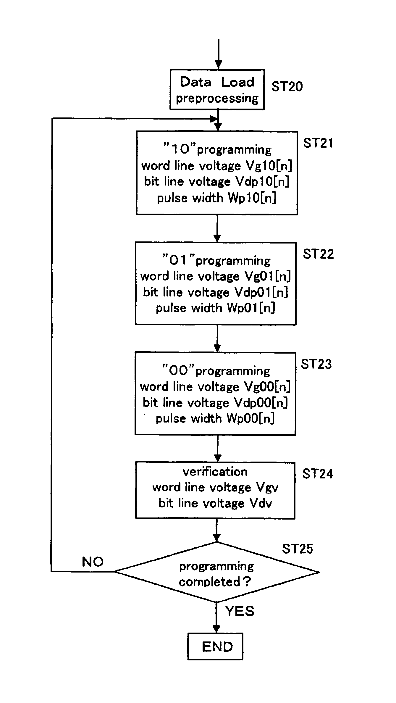
[0100]The case where there exist plural programming target memory cells on the same word line and their object memory states (threshold voltages) are different has been stated a little in the description of the first embodiment. This case will be described in detail with reference to FIG. 3. In a following description, assume that a set of memory cells to be programmed to the memory state “10” is A0, a set of memory cells to be programmed to the memory state “01” is B0 and a set of memory cells to be programmed to the memory state “00” is C0. In the meantime, the method according to the second embodiment of the present invention is executed with the inventive device 10 shown in FIGS. 1, 2 like the first embodiment.

[0101]From the initial state (ST20), first, the word line voltage is charged up to Vg10[0] and a bit line voltage Vdp10[0] is applied to all the memory cells included in A0, B0, C0 with a pulse width Wp10[0] so as to raise the threshold voltages of all the programming targ...

third embodiment

[0106]Next, an embodiment for the case where there exist plural programming target memory cells on the same word line and their object memory states (threshold voltages) are different will be described with reference to a flow chart of FIG. 8. Here, like the second embodiment, it is assumed that a set of the memory cells to be programmed to the memory state “10” is A0, a set of the memory cells to be programmed to the memory state “01” is B0 and a set of the memory cells to be programmed to the memory state “00” is C0. Because in the programming sequence shown in FIG. 8, a flow of steps ST30 to ST35 is equal to the steps ST20 to ST25 (see FIG. 3) of the second embodiment; therefore, its description will not be given here.

[0107]For sets A1, B1, C1 of programming target memory cells whose verifications do not pass in step ST35 of the first time, the word line voltage Vg10[1] (=Vg10[0]+ΔVg10[1]) (ΔVg10[1] is a larger voltage than 0 V) is set up again (ST36), a word line voltage Vg10[1]...


PUM


Abstract

This invention provides a programming method of a nonvolatile semiconductor device capable of programming multi-value data of three or more values rapidly. If between two threshold voltage ranges corresponding to respective memory states before and after programming, at least one threshold voltage range corresponding to other memory states exists in a programming target memory cell, a first programming step of applying at least one first program gate voltage corresponding to at least one of other memory states and a predetermined program drain voltage to a programming target memory cell is executed, then a second programming step of applying a second program gate voltage corresponding to a programmed state after programming and a predetermined program drain voltage is executed, and thereafter a verification step of verifying whether or not a program is made in a programming target memory cell is executed.

Description

BACKGROUND OF THE INVENTION[0001]1. Field of the Invention[0002]The present invention relates to a nonvolatile semiconductor memory device including a memory cell array constituted by arranging plural memory cells in the directions of rows and columns, the memory cells each having a charge accumulation region formed between a channel region and a control gate via insulation films and a programming method of the memory cell array. More particularly, the present invention relates to a nonvolatile semiconductor memory device whose memory cell is capable of storing data of three or more values.[0003]2. Description of the Related Art[0004]Conventionally as the most general flash memory of this kind of the nonvolatile semiconductor memory device, for example, EPROM thin oxide (ETOX, registered trade mark of Intel Corp.) type flash memory has been available.[0005]FIGS. 12A and 12B are a schematic sectional view of a memory cell transistor constituting a memory cell of an ETOX type flash me...

Claims


Application Information

Patent Timeline
Patent Type & Authority Patents(United States)
IPC IPC(8): G11C11/56G11C16/04G11C16/02G11C16/06
CPCG11C11/5628G11C16/0458
Inventor ONO, TSUYOSHIWATANABE, MASAHIKO
Owner SHARP KK
Why Eureka
Try Eureka