Semiconductor laser module

a laser module and semiconductor technology, applied in the direction of lasers, semiconductor laser structural details, semiconductor lasers, etc., can solve the problems of yield drop and insufficient stress reduction in the manufacture of semiconductor laser modules, and achieve the effect of sufficient stress reduction and improved production yield

Inactive Publication Date: 2005-11-01
LUMENTUM JAPAN INC
View PDF7 Cites 17 Cited by
  • Summary
  • Abstract
  • Description
  • Claims
  • Application Information

AI Technical Summary

Benefits of technology

[0008]An object of the present invention is to provide a semiconductor laser module permitting a sufficient reduction of the aforementioned stress and an improvement of the production yield.
[0010]This configuration makes possible a sufficient reduction of the stress and an improvement of the production yield.
[0013]This configuration makes possible a sufficient reduction of the stress and an improvement of the production yield.
[0017]This configuration makes possible a sufficient reduction of the stress and an improvement of the production yield.

Problems solved by technology

However, the present inventors made research work focusing on the thickness of the submount taken up in JP-A-5-299699 and on the combined thickness of the semiconductor laser chip and the submount taken up in JP-A-2001-168445, and found that stress cannot always be sufficiently reduced merely by adjusting the thickness of the submount.
If the stress reduction is insufficient, such defects as current threshold fluctuations or kinks will arise, resulting in a problem of a yield drop in the manufacture of semiconductor laser modules.

Method used


Image

  • Semiconductor laser module
  • Semiconductor laser module
  • Semiconductor laser module

Examples


Embodiment Construction

[0031]The structure of a semiconductor laser module according to a first preferred embodiment of the present invention, will be described below with reference to FIG. 1 through FIG. 8.

[0032]First will be described the structure of the semiconductor laser module embodying the invention in this mode with reference to FIG. 1.

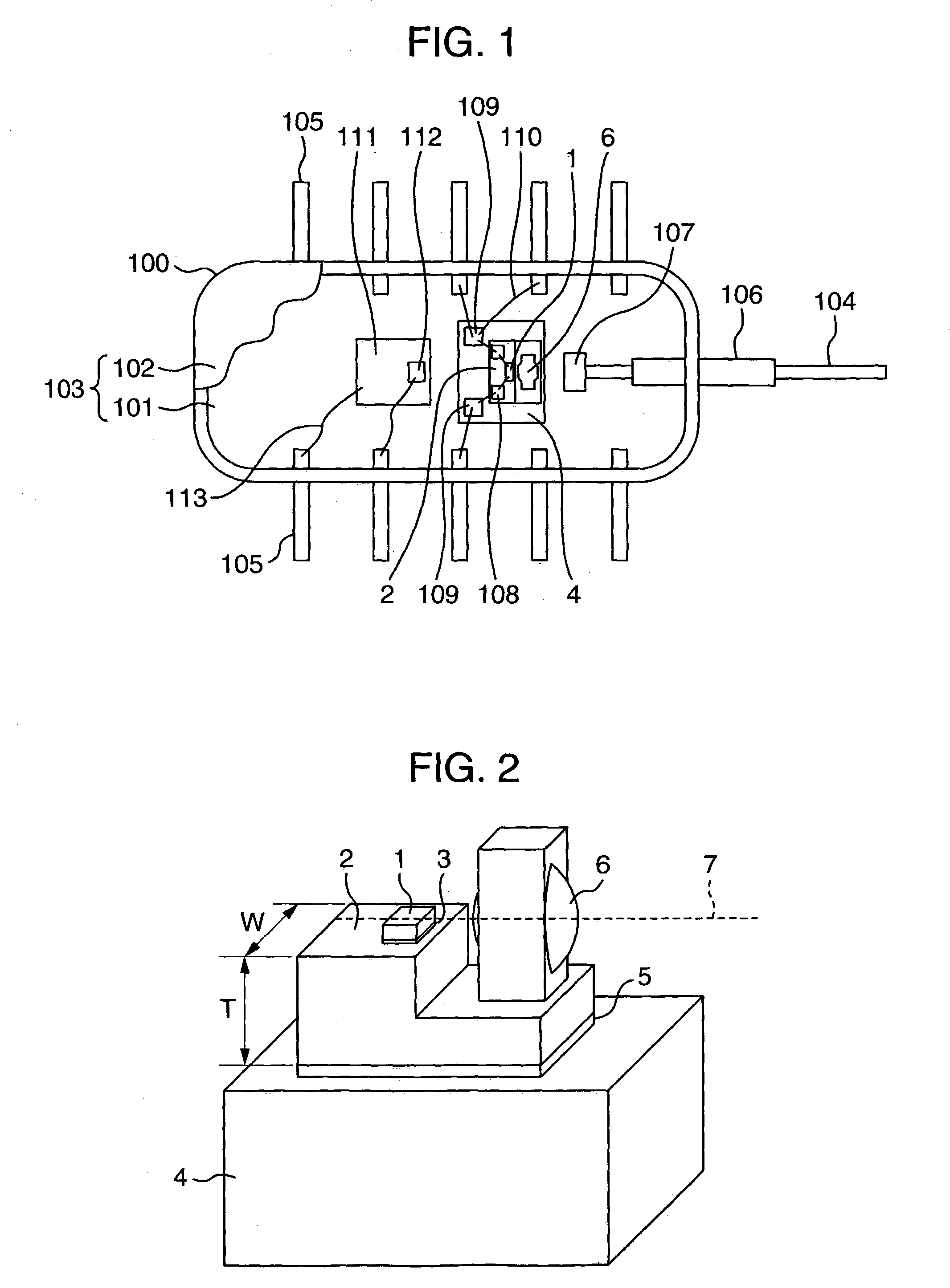
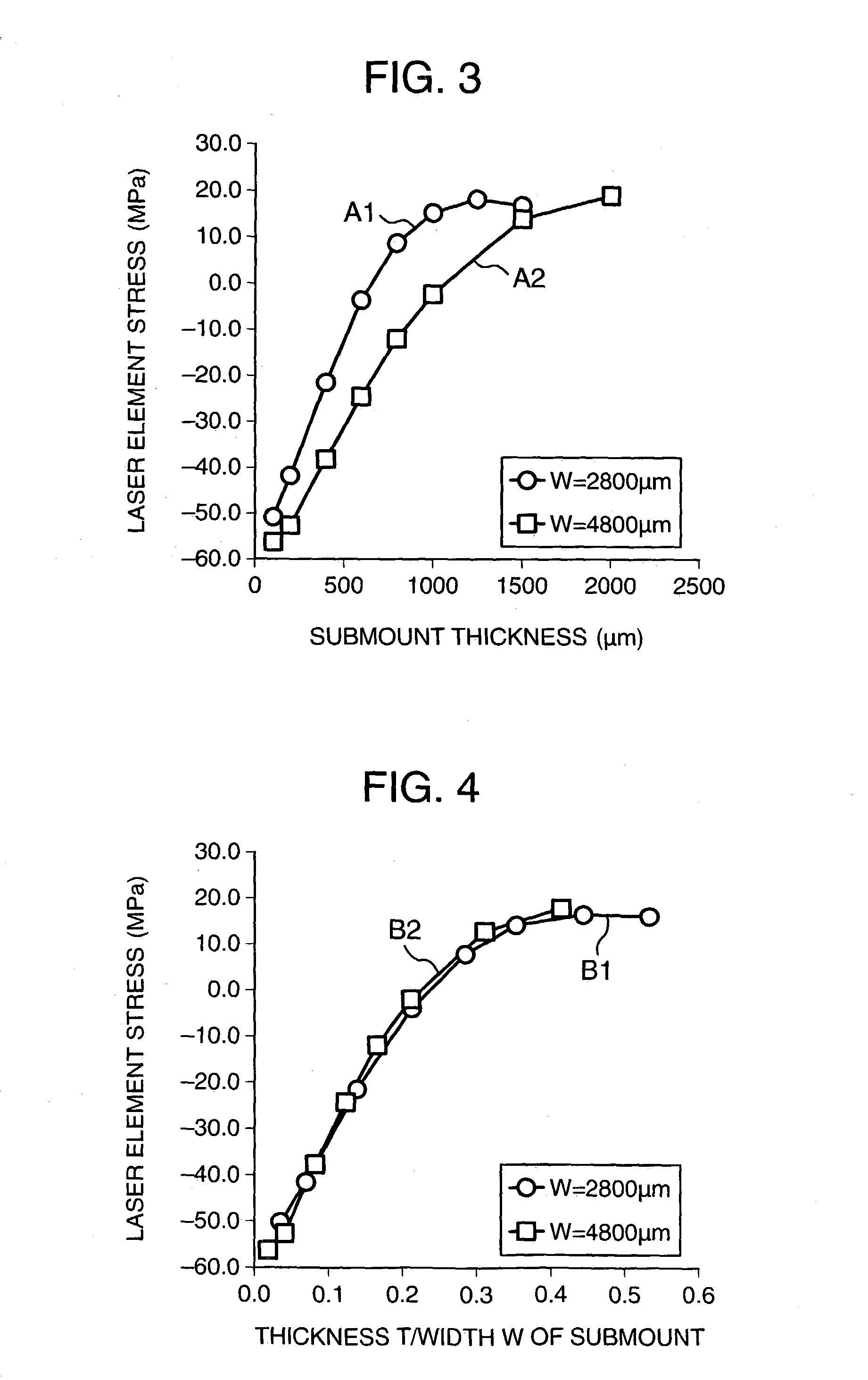
[0033]FIG. 1 shows a top view of essential parts of the structure of the semiconductor laser module according to the first preferred embodiment of the invention.

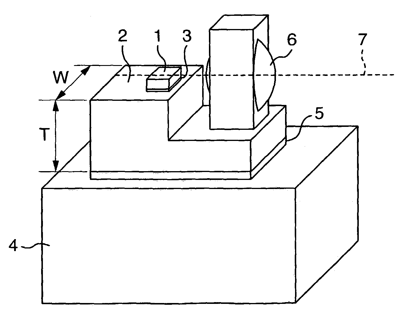
[0034]A semiconductor laser module 100 has a package 103 consisting, for instance, of a box-shaped package body 101 and a lid 102. The semiconductor laser module 100 further has an optical cable (optical fiber) 104 extending in and out of the package 103. The optical cable 104 is inserted into a guide pipe 106 penetrating the package body 101 and fixed with a bonding agent (not shown).

[0035]On the top face of the bottom of the package body 101 at the center is mounted a semiconductor laser element 1 with a ...


PUM


Abstract

In a semiconductor laser module, in order to sufficiently reduce the thermal stress arising in a due to the bonding of elements when they are packaged and to improve the yield of production, the semiconductor laser module is provided with a semiconductor laser element, a submount bonded to the semiconductor laser element with a solder layer in-between and thereby mounted with it, and a base mounted with this submount with another solder layer in-between. Herein, T / W≧0.15 holds, where W is the width of the submount in the direction orthogonal to the optical axis of the semiconductor laser element and T is the thickness of the submount.

Description

BACKGROUND OF THE INVENTION[0001]1. Field of the Invention[0002]The present invention relates to a semiconductor laser module, and more particularly to a semiconductor laser module having a suitable structure for reducing thermal stress arising from bonding of elements at the time of packaging.[0003]2. Description of the Related Art[0004]In recent years, semiconductor laser elements for mounting on a semiconductor laser module for use in optical communication have come to require higher output and greater accuracy in wavelength. There is a further need to prevent deterioration in element performance in terms of the occurrence of kinks and an increase in current threshold and thereby to improve the production yield. To meet these requirements, it is necessary to reduce thermal stress that occurs when a semiconductor laser element is soldered onto a submount and the base.[0005]In view of this need, there is known a configuration, as described in JP-A-5-299699, in which a submount usin...

Claims


Application Information

Patent Timeline
Patent Type & Authority Patents(United States)
IPC IPC(8): H01S3/04H01S5/00H01S5/022H01S5/02H01S5/023
CPCH01S5/02252H01S5/005H01S5/02216H01S5/02236H01S5/02272H01S5/02326H01S5/0237H01S5/023H01S5/0233H01S5/0235H01S5/02253
Inventor MORIYA, HIROSHIASHIDA, KISHONIWA, YOSHIAKI
Owner LUMENTUM JAPAN INC
Why Eureka
Try Eureka