Memory device having a semiconducting polymer film

a technology of semiconducting polymer and memory device, which is applied in the field of memory device having a semiconducting polymer film, can solve the problems of increasing the cost of processing, affecting the reliability of the device, and achieving the typical storage capacity of only a few megabytes

Inactive Publication Date: 2005-11-08
HEWLETT PACKARD DEV CO LP
View PDF15 Cites 36 Cited by
  • Summary
  • Abstract
  • Description
  • Claims
  • Application Information

AI Technical Summary

Problems solved by technology

Solid state memory devices, typically, have read write speeds on the order of nanoseconds, however, storage capacities of only a few Megabyte are typically achieved.
The ability to manufacture high capacity storage systems is typically constrained by the need to utilize movable or rotating parts, which is a relatively slow process compared to electronic circuit technology.
In addition, reliability is an additional problem, in order to decrease the read write times the movable or rotating parts tend to be utilized at as highest speed as possible.
Further, if the electronic device is used in a portable application the shock resistance of the system is typically a limitation.
Power consumption, overall weight and size, and cost are also factors that limit storage systems.
Typically, silicon based memory devices involve complex architectures on single crystal semiconductor substrates, which results in higher cost.
In addition, such complex architecture, typically, result in a reduction in the number of logic cells per unit area of the semiconductor substrate, leading to a reduction in the data storage density for a given chip size.
Further, currently the fabrication of semiconducting circuits on polymer substrates, especially on flexible polymer substrates, is hindered by the typical harsh processing conditions for silicon-based devices such as high temperatures.
Thus, the semiconductor circuit elements are typically fabricated on semiconductor substrates such as single crystal silicon, and then separately mounted on the polymer substrate, requiring further interconnections, processing and cost.
However, this technology generally requires processing temperatures in the range of 300° C. to 400° C. that typically results in the melting or severe degradation of most polymer substrates.
There are a number of other problems in fabricating semiconducting circuits on polymer substrates.
In general, only a limited number of polymers, such as polyimides, are available that can withstand the temperatures utilized in fabricating silicon semiconducting circuits.
In addition, compatibility can be an issue; for example the difference in thermal expansion between silicon and polymers is large, typically resulting in thermal stress that can affect device performance.
Further, the deposition of silicon typically requires sophisticated and expensive equipment that requires a vacuum and is optimized for deposition on wafers.
These problems render impractical the manufacture of durable, lightweight, and low cost electronic memory devices.

Method used


Image

  • Memory device having a semiconducting polymer film
  • Memory device having a semiconducting polymer film
  • Memory device having a semiconducting polymer film

Examples


Embodiment Construction

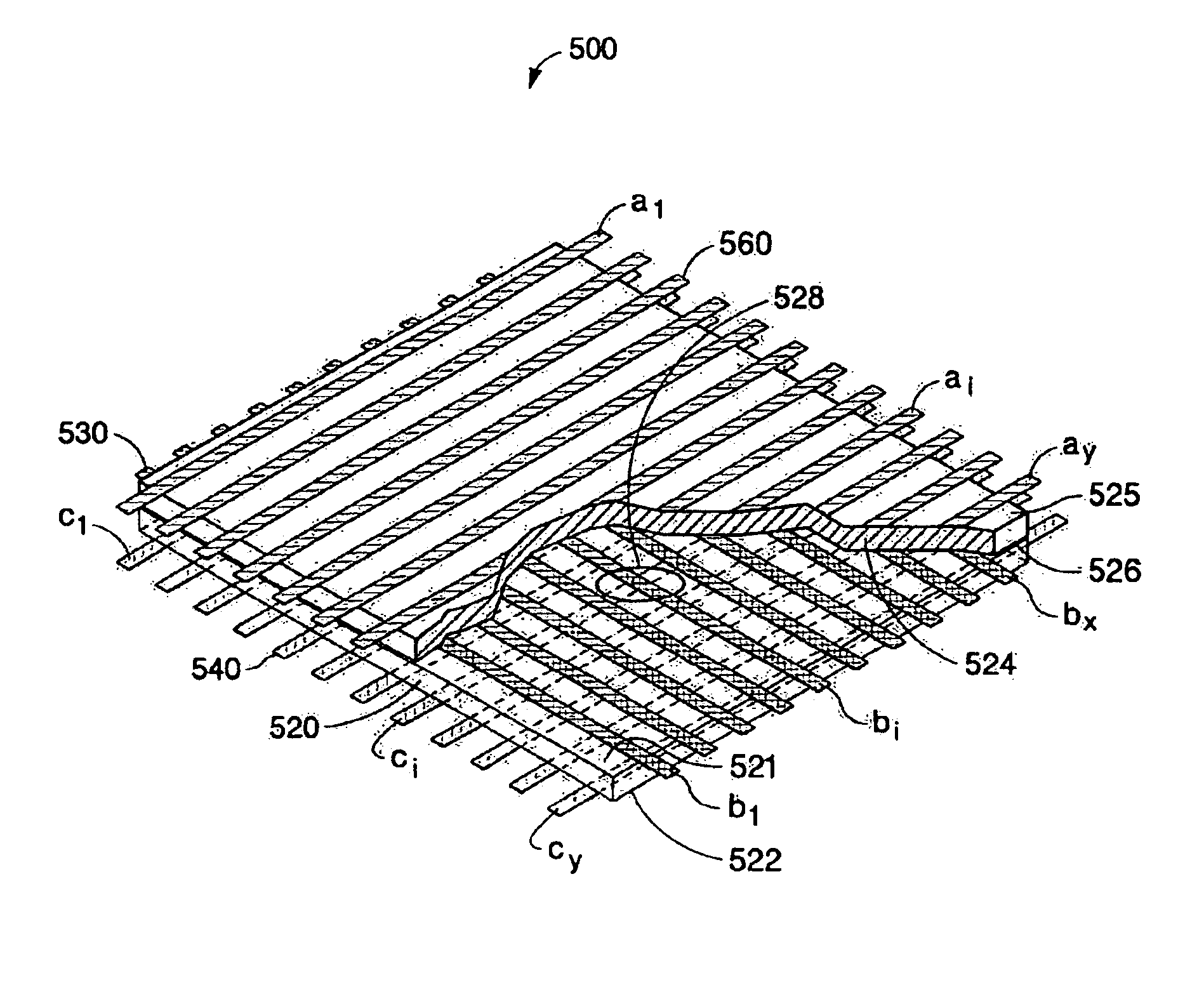
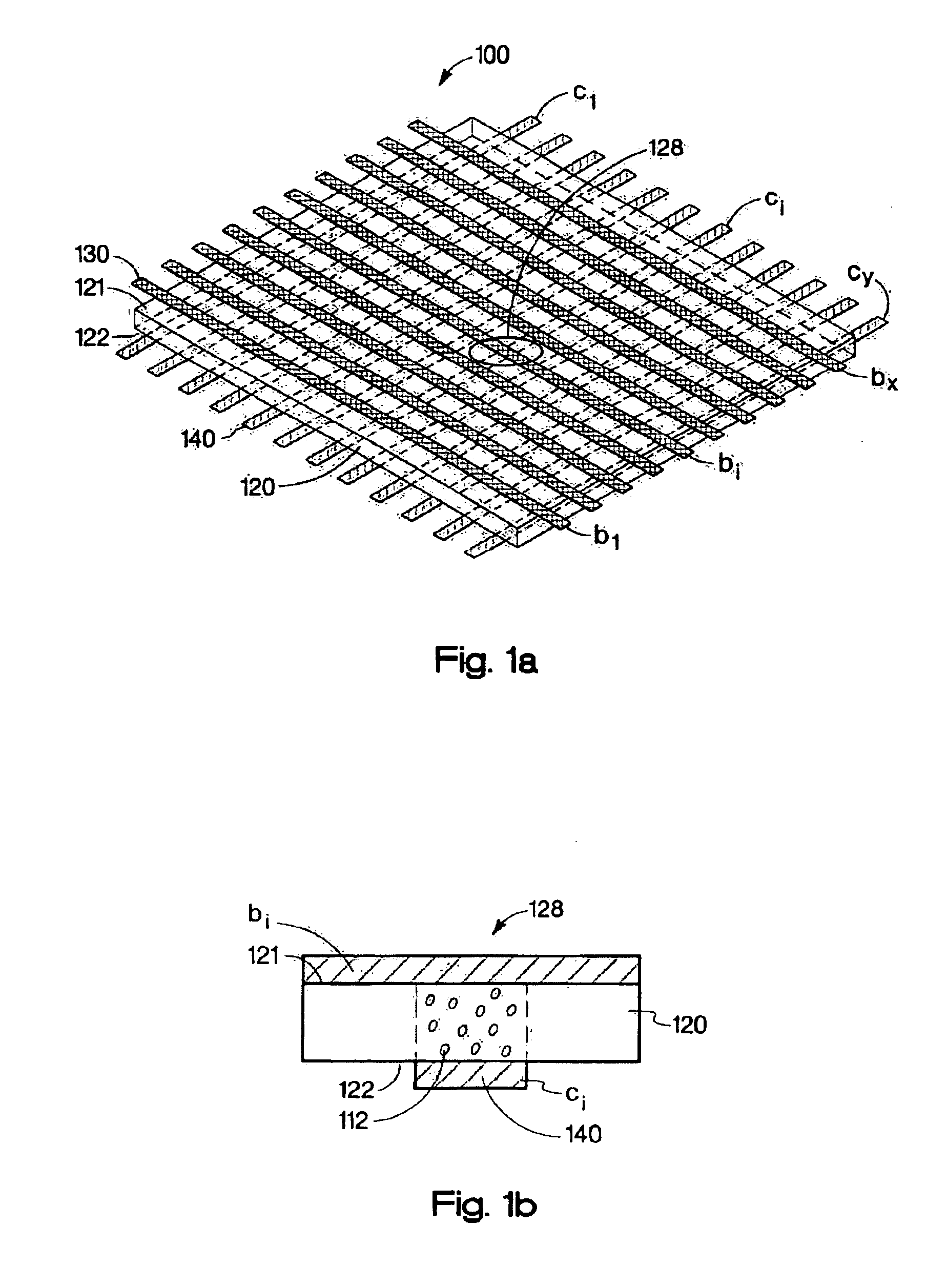
[0019]Referring to FIG. 1a, an exemplary embodiment of memory device 100 of the present invention is shown in a perspective view. In this embodiment, semiconducting polymer film 120 forms a layer that includes an organic dopant (see FIG. 1b). On the top surface, also referred to as first side 121, of semiconducting polymer film 120, a plurality of electrical conductors 130 are formed and are denoted as bj. Electrical conductors 130 are substantially parallel to each other. On the bottom surface, also referred to as second side 122, of semiconducting polymer film 120 are formed a corresponding plurality of electrical conductors 140 that are substantially parallel to each other and are substantially mutually orthogonal to electrical conductors 130. The electrical conductors 140 are denoted as ci. The combination of electrical conductors 130 and 140 form a planar orthogonal x, y matrix. Logic cell 128 includes the volume of semiconducting polymer film 120 between any two intersecting e...


PUM

PropertyMeasurementUnit
temperaturesaaaaaaaaaa
thicknessaaaaaaaaaa
thicknessaaaaaaaaaa

Abstract

A memory device includes a semiconducting polymer film, which includes an organic dopant. The semiconducting polymer film has a first side and a second side. The memory device also includes a first plurality of electrical conductors substantially parallel to each other coupled to the first side of the semiconducting polymer layer, and a second plurality of electrical conductors substantially parallel to each other, coupled to the second side of the semiconducting polymer layer. The first and second pluralities of electrical conductors are substantially mutually orthogonal to each other. Further, an electrical charge is localized on the organic dopant.

Description

[0001]This application is a divisional of U.S. application Ser. No. 10 / 171,738 filed Jun. 14,2002 now U.S. Pat. No. 6,828,685.BACKGROUNDDescription of the Art[0002]Over the past few years, the demand for ever cheaper and lighter weight portable electronic devices has led to a growing need to manufacture durable, lightweight, and low cost electronic circuits including high density memory chips. Solid state memory devices, typically, have read write speeds on the order of nanoseconds, however, storage capacities of only a few Megabyte are typically achieved. On the other hand, mass storage devices, which usually have a rotating medium, have the capability of storing a few Gigabytes of data; however, they have read write speeds of the order of only milliseconds.[0003]The ability to manufacture high capacity storage systems is typically constrained by the need to utilize movable or rotating parts, which is a relatively slow process compared to electronic circuit technology. In addition,...

Claims


Application Information

Patent Timeline
Patent Type & Authority Patents(United States)
IPC IPC(8): G11C13/02G11C11/34H01L51/30H01L27/28H01L51/05H01L27/10H01L51/00
CPCG11C11/34G11C13/0014G11C13/0016G11C13/0069H01L27/285B82Y10/00G11C2013/009G11C2213/77G11C2213/81H01L27/28H01L51/0042H01L51/005H01L51/0078H01L51/0094H01L2924/0002H01L2924/00H10K19/202H10K19/00H10K85/146H10K85/60H10K85/311H10K85/40H01L27/12H10K10/00
Inventor STASIAK, JAMES
Owner HEWLETT PACKARD DEV CO LP
Why Eureka
Try Eureka