Electronic components such as thin array plastic packages and process for fabricating same

a technology of electronic components and plastic packages, applied in the field of unique construction and process for fabricating electronic components, can solve the problem of limiting the packaging density of such prior art devices

Inactive Publication Date: 2005-11-15
UTAC HEADQUARTERS PTE LTD
View PDF30 Cites 86 Cited by
  • Summary
  • Abstract
  • Description
  • Claims
  • Application Information

AI Technical Summary

Problems solved by technology

The inner leads terminate in outer leads that are bent down to contact a mother board, thereby limiting the packaging density of such prior art devices.

Method used


Image

  • Electronic components such as thin array plastic packages and process for fabricating same
  • Electronic components such as thin array plastic packages and process for fabricating same
  • Electronic components such as thin array plastic packages and process for fabricating same

Examples


Embodiment Construction

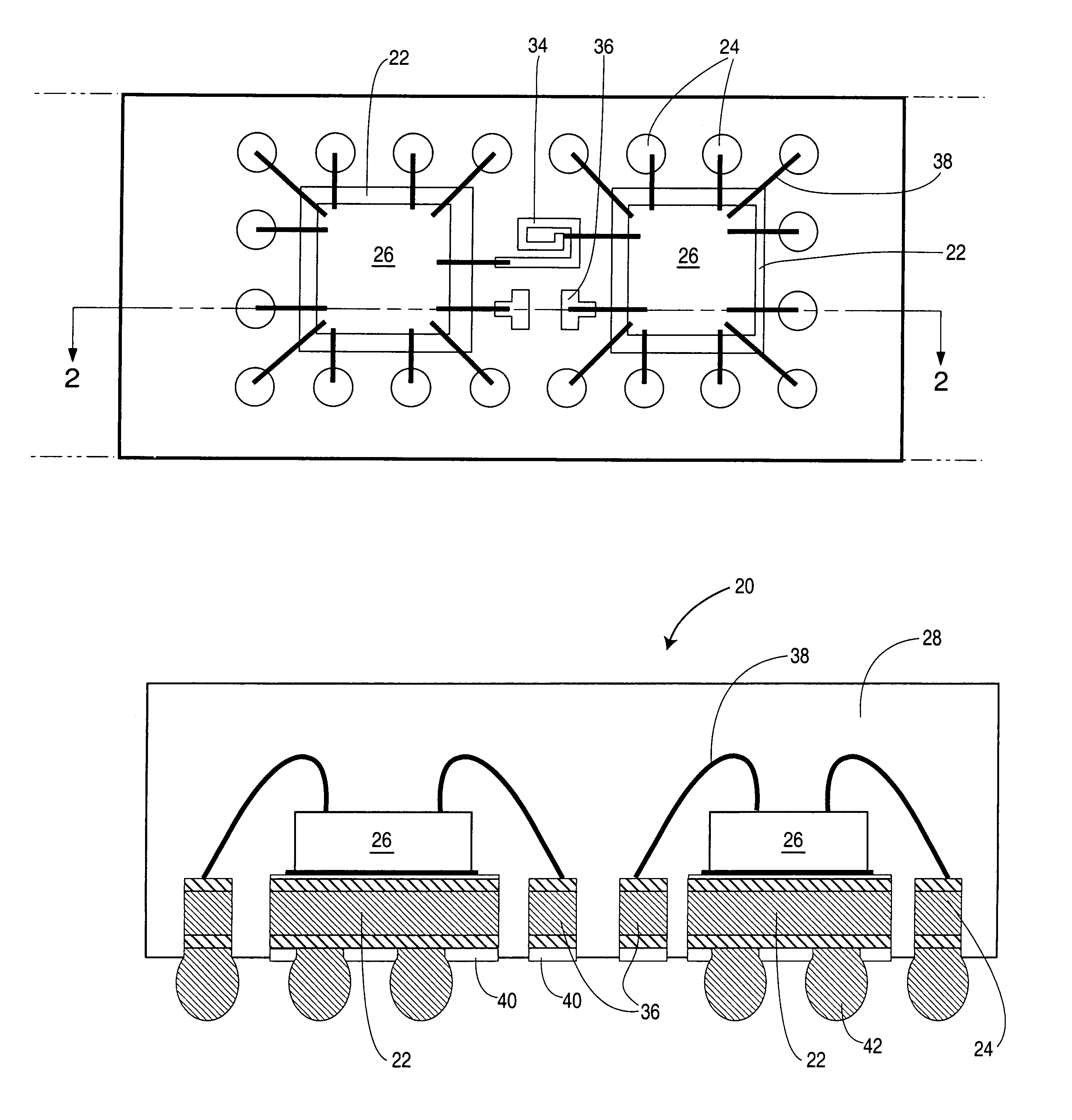
[0022]Reference is made to FIGS. 1A to 1K to describe processing steps for fabricating an integrated circuit package according to a first embodiment of the present invention, indicated generally by the numeral 20. The integrated circuit package 20 has a plurality of components including at least one die attach pad 22, at least one row of contact pads 24 and at least one additional electronic component. The plurality of components are comprised of a plurality of metallic layers. At least one semiconductor die 26 is mounted to a respective one of the at least one die attach pad 22 and electrically connected to the ones of the contact pads 24 and to the at least one additional electronic component. An overmold 28 covers the at least one semiconductor die 26 and the plurality of components.

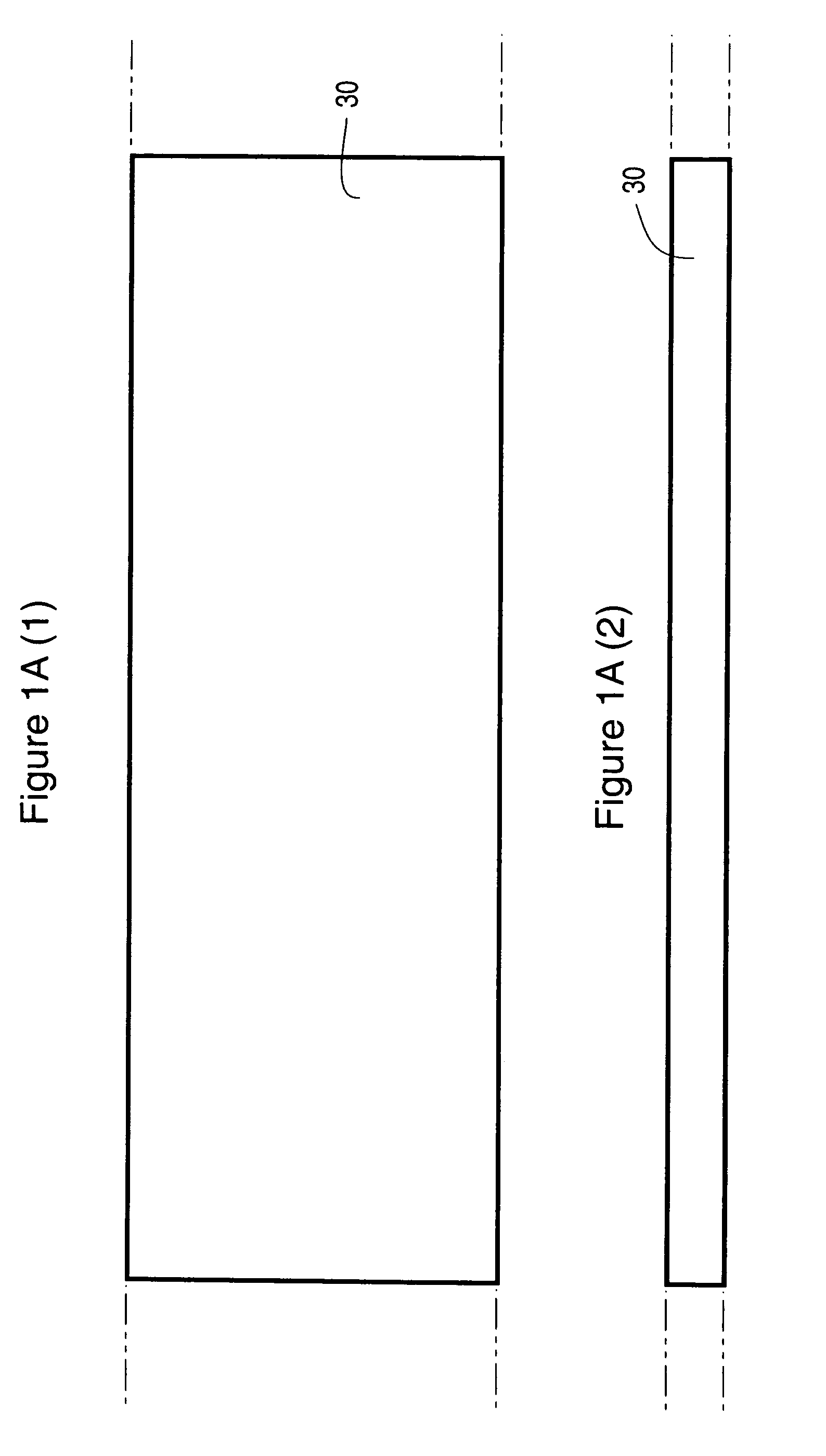
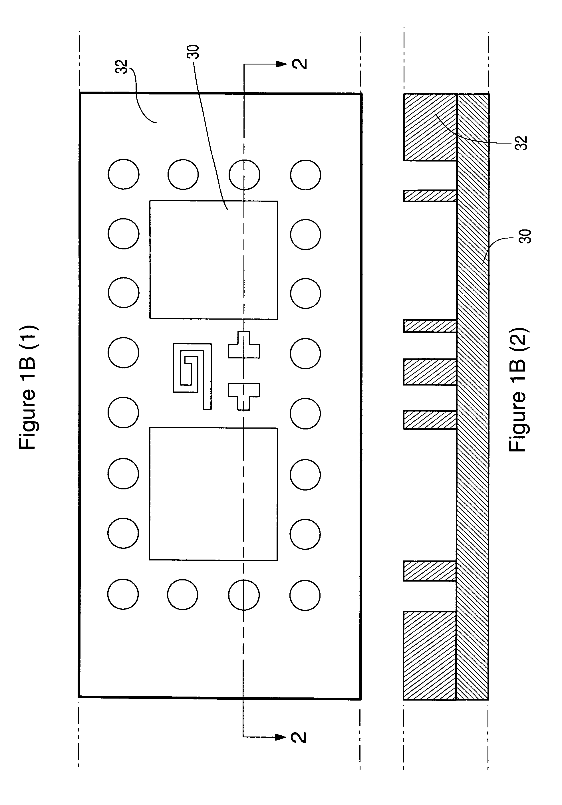
[0023]The processing steps for fabricating the integrated circuit (IC) package 20 will now be described with reference to FIGS. 1A to 1K. Reference is first made to FIG. 1A(1), which shows a top view ...


PUM


Abstract

A process for fabricating an integrated circuit package includes establishing a plating mask on a first surface of a metal carrier. The plating mask defines a plurality of components including a die attach pad, at least one row of contact pads and at least one additional electronic component. A plurality of metallic layers are deposited on exposed portions of the first surface of the metal carrier. The plating mask is stripped from the metal carrier, leaving the plurality of metallic layers in the form of the plurality of components. A semiconductor die is mounted to die attach pad and pads of the semiconductor die are electrically connected to ones of the contact pads and to the additional electronic component. The first surface of the metal carrier is overmolded to encapsulate the plurality of components and the semiconductor die and the metal carrier is etched away.

Description

CROSS REFERENCE TO RELATED APPLICATION[0001]This is a continuation-in-part of U.S. patent application Ser. No. 09 / 802,678 filed Mar. 9, 2001 which is a continuation-in-part of of U.S. patent application Ser. No. 09 / 288,352, filed Apr. 8, 1999, now U.S. Pat. No. 6,498,099, which is a continuation-in-part of U.S. patent application Ser. No. 09 / 095,803, filed Jun. 10, 1998, now U.S. Pat. No. 6,229,200.FIELD OF THE INVENTION[0002]The present invention relates generally to electronic components and more particularly to a unique construction and process for fabricating electronic components such as thin array plastic packages, inductors and capacitors.BACKGROUND OF THE INVENTION[0003]According to well known prior art IC (integrated circuit) packaging methodologies, semiconductor dice are singulated and mounted using epoxy or other conventional means onto respective die attach pads (attach paddles) of a leadframe strip. Traditional QFP (Quad Flat Pack) packages incorporate inner leads whic...

Claims


Application Information

Patent Timeline
Patent Type & Authority Patents(United States)
IPC IPC(8): H01L21/44H01L21/02H01L21/48H01L21/68H01L23/31H05K1/18H05K3/20
CPCH01L21/4832H01L21/568H01L21/6835H01L23/3107H01L2224/48091H01L2224/48247H01L2924/01046H01L2924/01078H01L2924/01079H01L2924/19041H05K1/185H05K1/187H05K3/205H01L2924/00014H01L24/48H01L2224/48257H01L2224/45144H01L2924/00H01L2224/45124H01L2224/45147H01L24/45H01L2924/14H01L2924/181H01L2924/18165H01L2924/00015H01L2224/05599H01L2924/00012
Inventor FAN, CHUN HOTSANG, KWOK CHEUNG
Owner UTAC HEADQUARTERS PTE LTD
Why Eureka
Try Eureka