Magnetic memory device and method of manufacturing the same

a memory device and magnetic technology, applied in the direction of magnetic bodies, semiconductor/solid-state device details, instruments, etc., can solve the problems of low vapor pressure, difficult processing in the ordinary semiconductor manufacturing process, and insufficient chemical reaction ra

Inactive Publication Date: 2005-11-15
KIOXIA CORP
View PDF5 Cites 56 Cited by
  • Summary
  • Abstract
  • Description
  • Claims
  • Application Information

AI Technical Summary

Problems solved by technology

However, halides of 3d transition metals, such as Fe, Ni, Co and Cu, used in the formation of the MTJ element, have a low vapor pressure, and it is difficult to be processed in the ordinary semiconductor manufacturing process.
In this method, however, the chemical reaction rate is insufficient, and the process inevitably involves physical sputtering using a reaction gas.
Thus, this method has not yet been put to practical use.
It has turned out that in some cases, the residual film has electrical conductivity, and it may short-circuit the insulating barrier film, leading to initial defects of the MRAM cell.

Method used


Image

  • Magnetic memory device and method of manufacturing the same
  • Magnetic memory device and method of manufacturing the same
  • Magnetic memory device and method of manufacturing the same

Examples


second embodiment

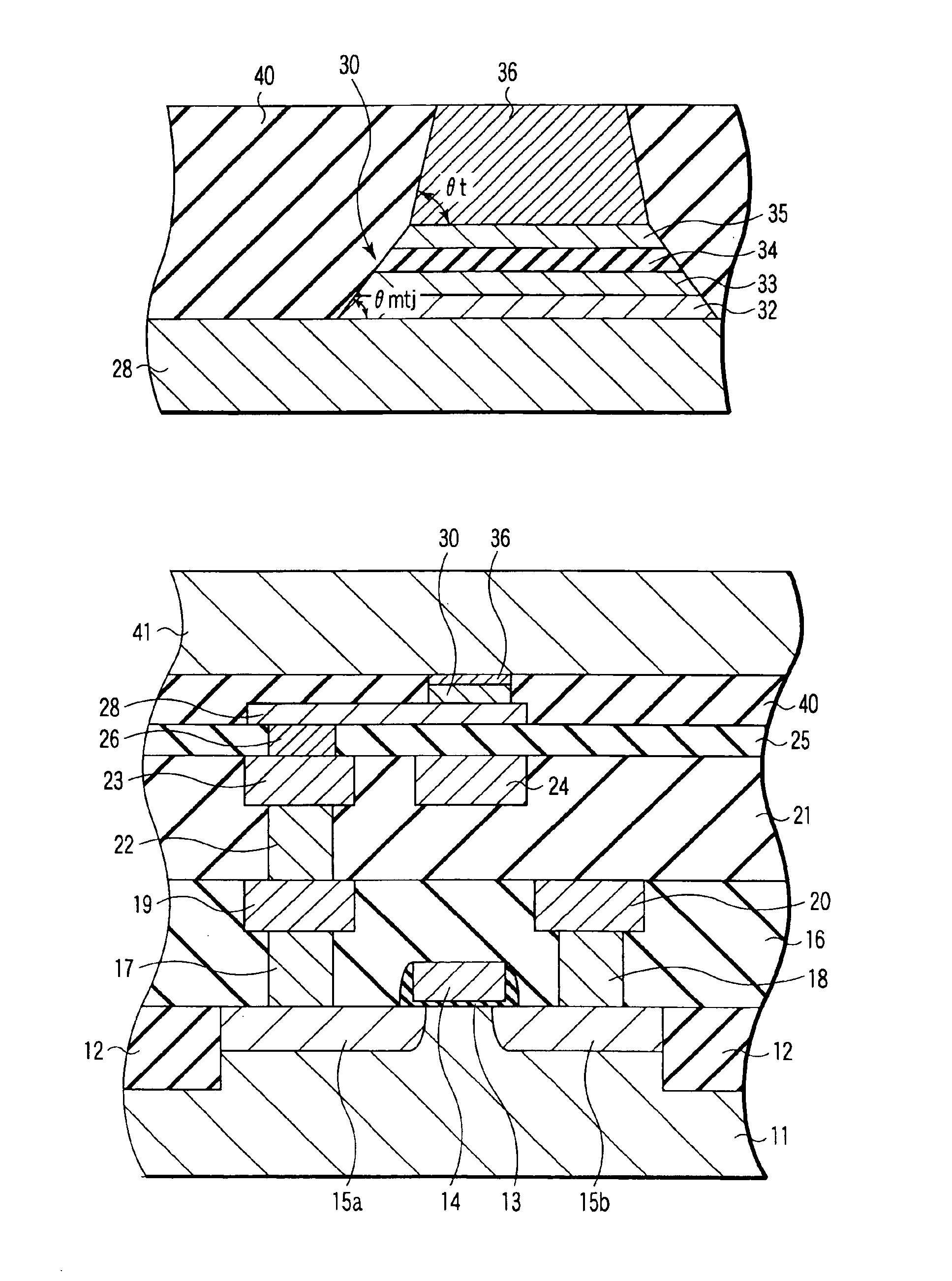
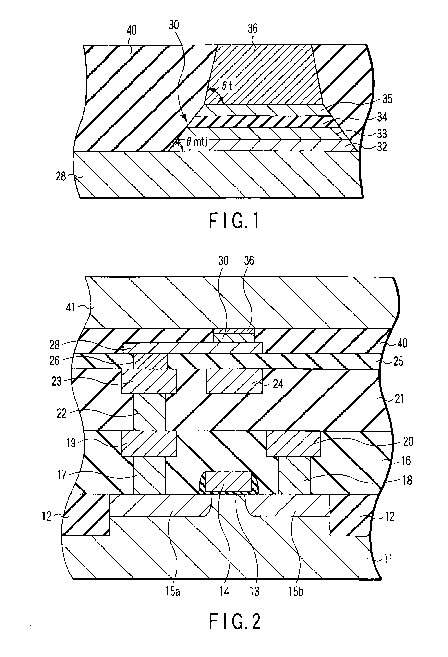
[0175]In the second embodiment, the taper angle of the hard mask 36 is made greater than that of the MTJ element 30. Thereby, the insulation film on the side wall of the hard mask remains due to the angle dependency of the etching rate, which quickly decreases on the large incidence angle side. Therefore, the metallic contamination source to the side wall of the MTJ element can be suppressed.

[0176]On the other hand, as will be described below, the taper angle of the hard mask may be made smaller than the taper angle of the side wall of the MTJ element.

[0177]A magnetic memory device according to a third embodiment of the present invention and a method of manufacturing the magnetic memory device will now be described referring to FIGS. 17A through 18C. In the third embodiment, the parts common to those in the above-described second embodiment are denoted by like reference numerals, and a detailed description thereof is omitted.

[0178]In FIG. 17A, a lower electrode 28, a magneto-resisti...
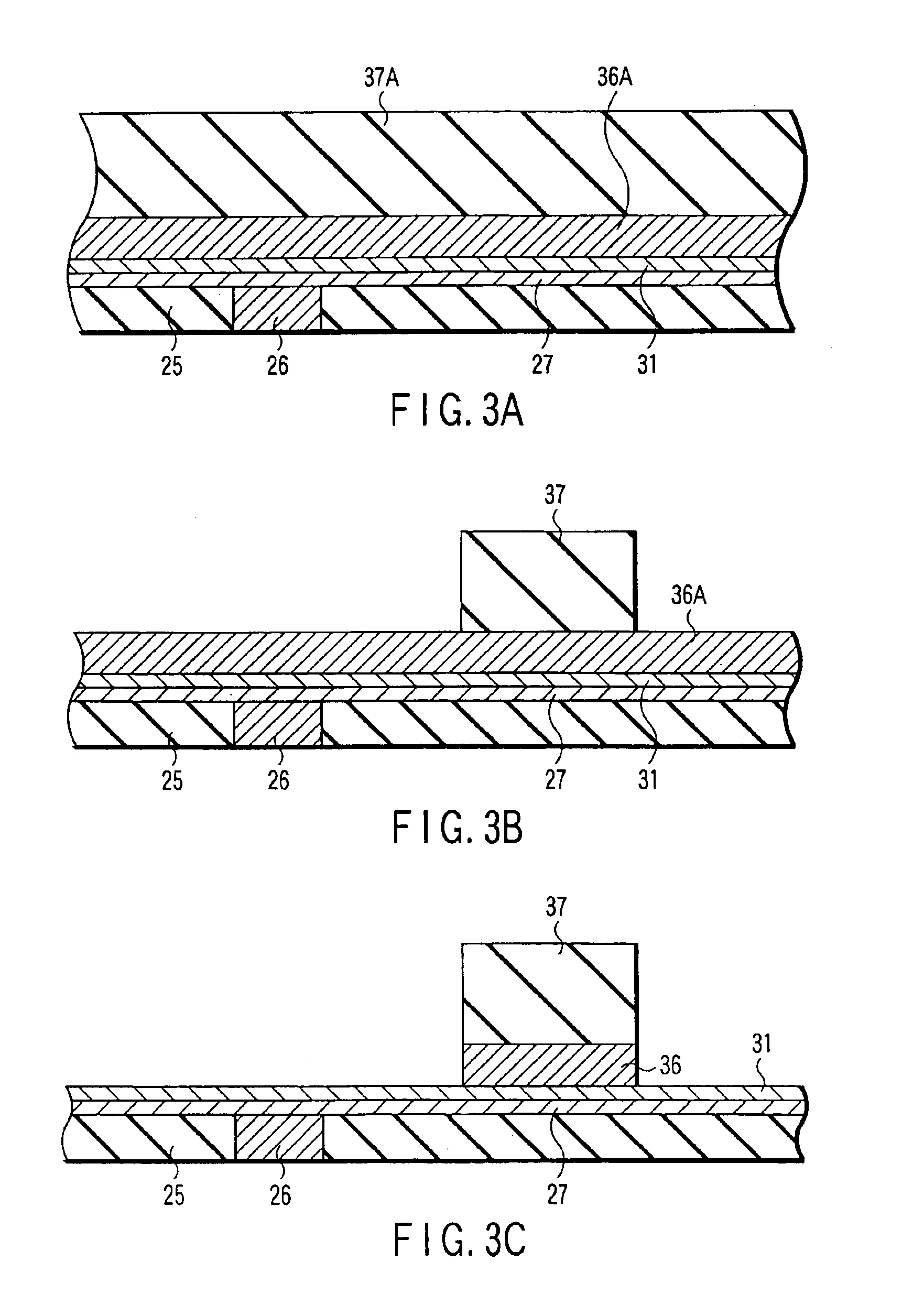
third embodiment

[0183]In the third embodiment, the etching for forming the MTJ element 30 shown in FIG. 18A is effected by Ar ion beam etching using the hard mask 36 as a mask. The Ar ion beam etching is performed, for example, under conditions that the voltage of the ion beam is 400 V, the ion beam current amount IB=100 mA, the ion acceleration voltage VB=100 V, and the incidence angle θ to the normal line of the substrate is about 45°. A contaminant conductive film (not shown) is formed on the taper surface of the MTJ element 30.

[0184]Thereafter, as shown in FIG. 18B, a protection film 39 serving as an insulation film is deposited by, e.g. reactive sputtering, on the entire surfaces of the lower electrode 28, MTJ element 30 and hard mask 36.

[0185]In particular, in order to enhance the coverage on the side surface of the hard mask 36, the protection film 39 is formed by bias sputtering, using, e.g. SiO2, to a thickness of about 80 nm. Next, Ar ion etching is performed over the entire upper surface...


PUM

PropertyMeasurementUnit
taper angleaaaaaaaaaa
angleaaaaaaaaaa
angleaaaaaaaaaa

Abstract

A method of manufacturing a magnetic memory device includes forming an insulation layer on a substrate, forming a lower electrode on the insulation layer, forming a magneto-resistive film on an upper surface of the lower electrode, the magneto-resistive film including an insulation barrier layer and a plurality of magnetic films stacked on both sides of the insulation barrier layer, stacking a mask layer on the magneto-resistive film, performing ion etching on the magneto-resistive film, using the mask layer as a mask, thereby forming a magneto-resistive element, forming an insulation film on upper surfaces of the mask, the magneto-resistive element and the lower electrode, and etching the insulation film with an ion beam such that a side surface of the magneto-resistive element is exposed.

Description

CROSS-REFERENCE TO RELATED APPLICATIONS[0001]This application is based upon and claims the benefit of priority from the prior Japanese Patent Application No. 2003-200413, filed Jul. 23, 2003, the entire contents of which are incorporated herein by reference.BACKGROUND OF THE INVENTION[0002]1. Field of the Invention[0003]The present invention relates to a magnetic memory device of a magnetic random access memory (hereinafter referred to as “MRAM”), and more particularly to a magnetic memory device using a magneto-resistive element and a method of manufacturing the magnetic memory device.[0004]2. Description of the Related Art[0005]The MRAM is a generic term of a nonvolatile solid-state memory which can randomly rewrite, store and read information as an information recording medium, making use of a variation in resistance value of a barrier layer due to a change in direction of magnetization of ferromagnetic layers. In general, a memory cell of the MRAM has a stacked structure of a pl...

Claims


Application Information

Patent Timeline
Patent Type & Authority Patents(United States)
IPC IPC(8): G11C11/00G11C11/02H01L21/336H01L29/76H01L29/66H01L21/02H01L43/00H01L27/00H01L27/105H01L43/08H01L43/12H01L31/115H01L31/119C23F4/00H01F10/32H01F41/30H01L21/8246H01L27/22
CPCB82Y10/00B82Y25/00B82Y40/00C23F4/00H01F41/308H01L27/228H01L43/08H01L43/12H01F10/3254H10B61/22H10N50/10H10N50/01H01L27/105
Inventor NAKAJIMA, KENTAROAMANO, MINORUUEDA, TOMOMASATAKAHASHI, SHIGEKI
Owner KIOXIA CORP
Why Eureka
Try Eureka