System and method for erase test of integrated circuit device having non-homogeneously sized sectors

a technology of integrated circuit devices and sectors, applied in the field of testing integrated circuit devices, can solve problems such as device rejection

Inactive Publication Date: 2005-11-15
MONTEREY RES LLC
View PDF9 Cites 7 Cited by
  • Summary
  • Abstract
  • Description
  • Claims
  • Application Information

AI Technical Summary

Problems solved by technology

If it does, the device is rejected.

Method used


Image

  • System and method for erase test of integrated circuit device having non-homogeneously sized sectors
  • System and method for erase test of integrated circuit device having non-homogeneously sized sectors
  • System and method for erase test of integrated circuit device having non-homogeneously sized sectors

Examples


Embodiment Construction

”.

BRIEF DESCRIPTION OF DRAWINGS

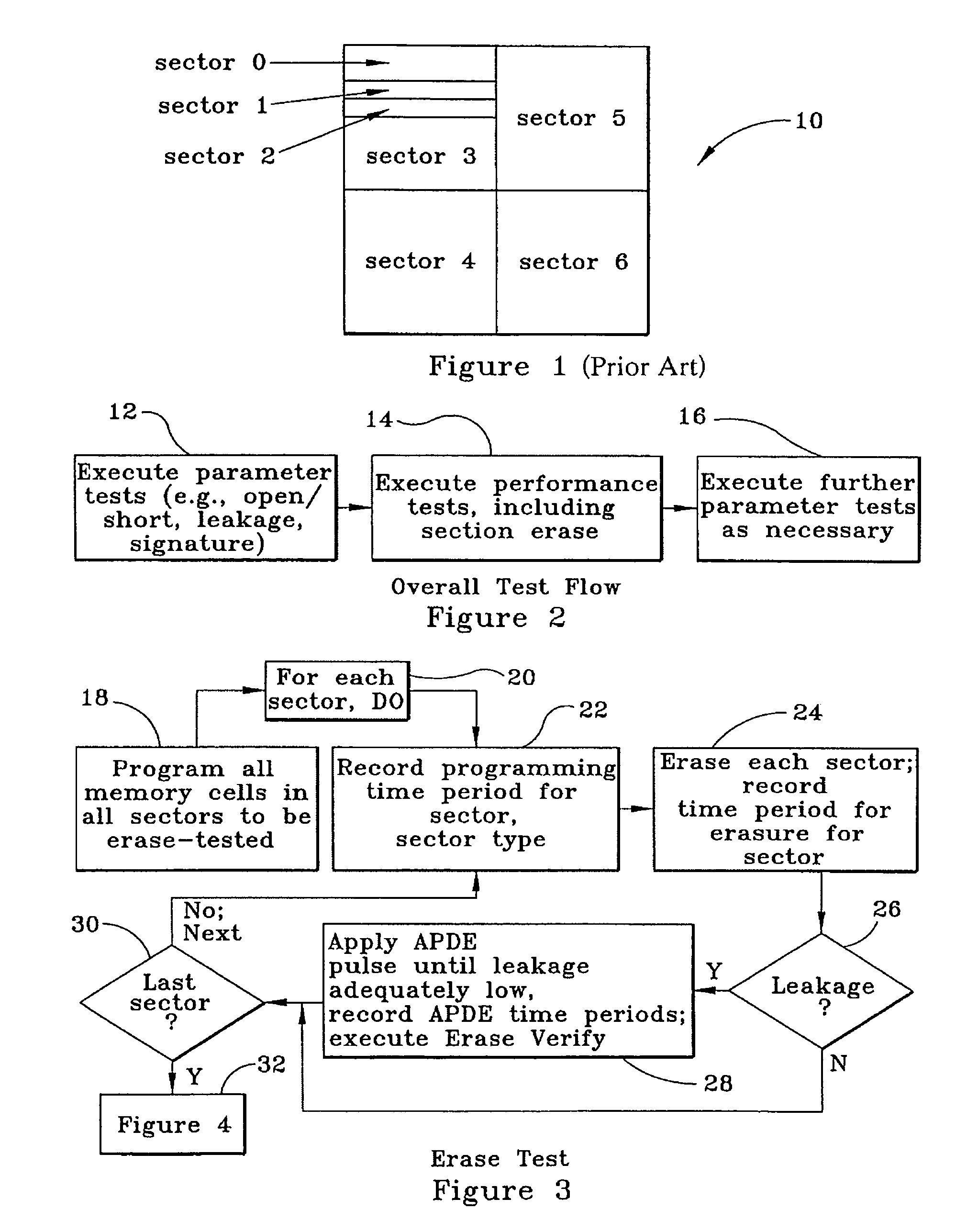
[0011]FIG. 1 is a schematic view of a flash memory device having uniform sectors and non-uniform sectors;

[0012]FIG. 2 is a flow chart of the overall logic of the present invention;

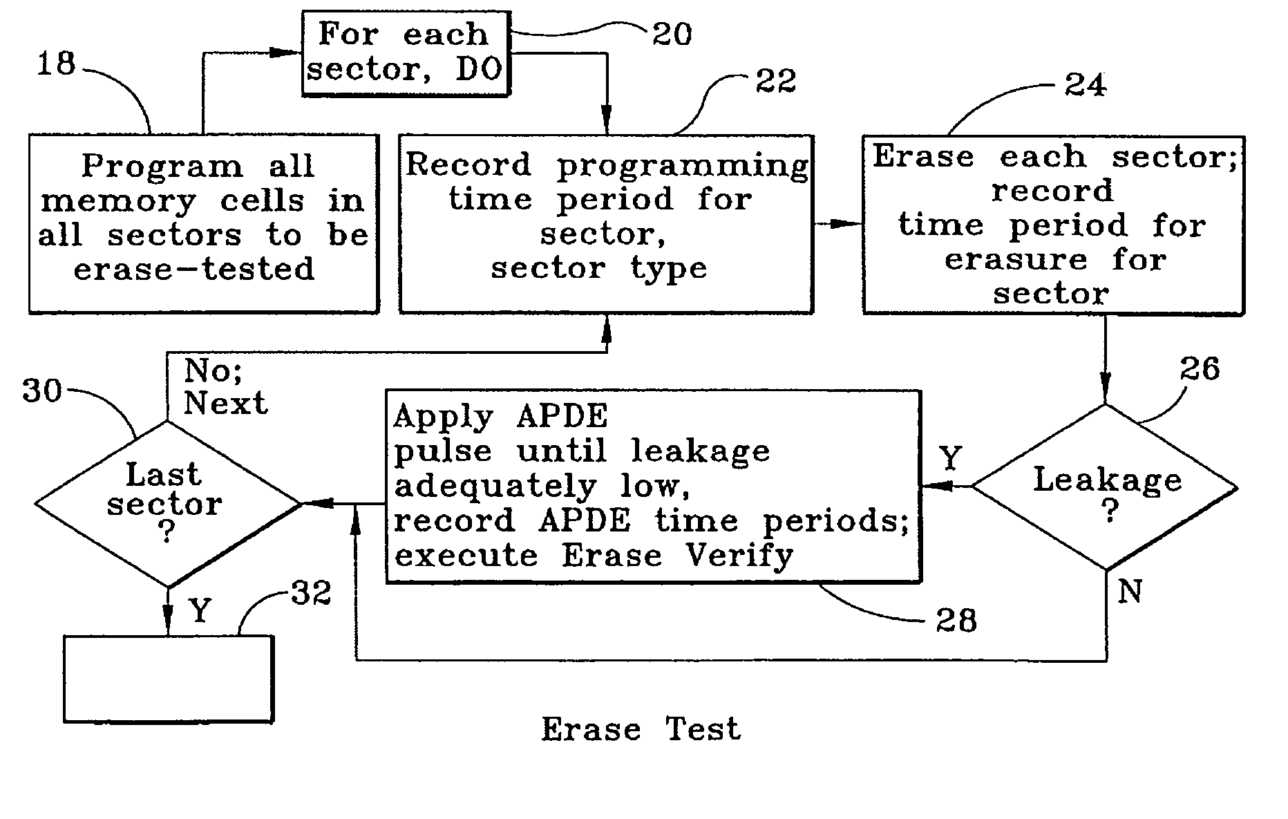
[0013]FIG. 3 is a flow chart of the erase test logic; and

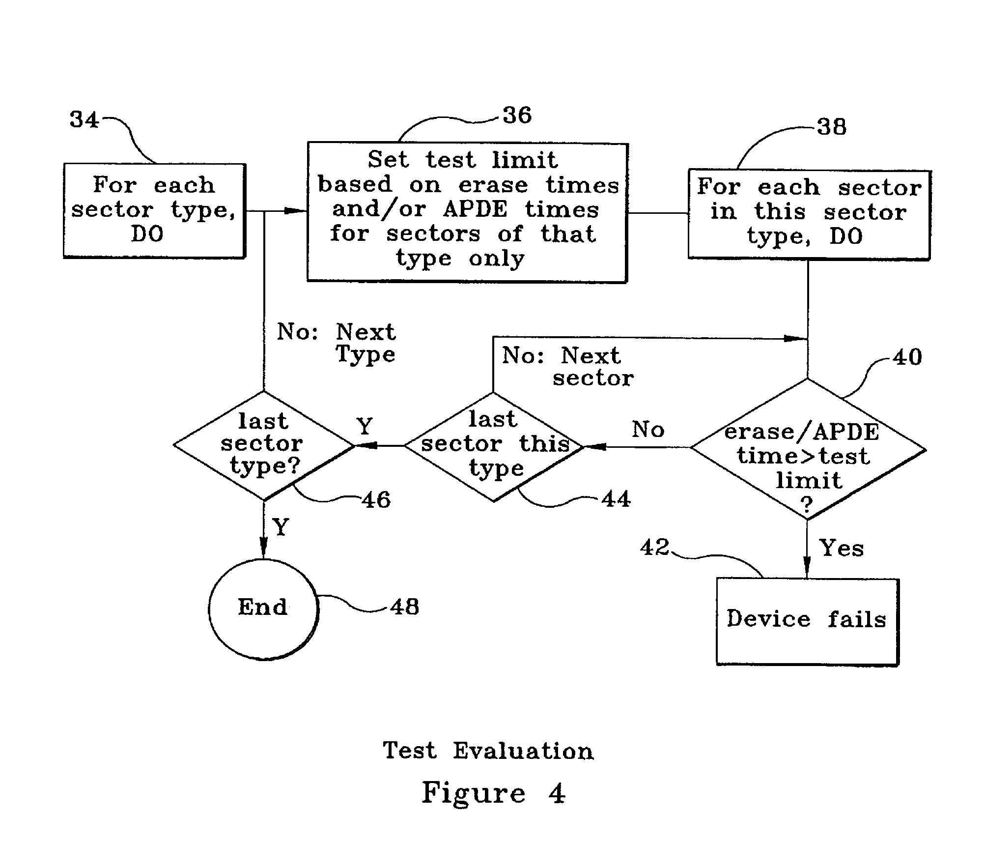
[0014]FIG. 4 is a flow chart of the erase test evaluation logic.

DETAILED DESCRIPTION OF THE INVENTION

[0015]Referring initially to FIG. 1, a semiconductor device, more specifically a bootable device, and still more specifically a flash memory device, is shown and generally designated 10. As shown, the device includes plural sectors. The sectors labeled “sector 5”, “sector 6”, and “sector 4” are all uniformly sized, relatively large sectors. This means they all have the same number of memory cells. On the other hand, the sectors labeled “sector 0”, “sector 1”, “sector 2”, and “sector 3” are non-uniformly sized, compared to the uniformly sized sectors, are relatively small and, hence, can be referred to as “baby sectors”. ...


PUM


Abstract

A system and method for testing a flash memory device having uniform sectors and smaller, “boot” sectors includes determining uniform and boot test limits. The uniform and boot test limits are determined based on average erase and APDE time periods of the uniform and boot sectors, respectively. In this way, the erase test results for each sector type is compared against test limits that are based only on that sector type, thereby avoiding excessive false rejects.

Description

TECHNICAL FIELD[0001]The present invention relates generally to testing integrated circuit devices such as flash memory devices.BACKGROUND OF THE INVENTION[0002]Semiconductor devices, including integrated circuit devices such as boot-type devices, are tested prior to shipment to ensure quality control. In the case of boot-type devices known as flash memory devices, the testing can include parametric tests, including testing for short circuits, open circuits, various leakage tests, and various signature tests. Also, the testing can include various performance or functional tests, such as speed tests and erase time tests. Of importance to the present invention is testing a device for erase time.[0003]Specifically, to determine whether a device can be erased adequately, each sector in the device is programmed, and then the device is erased, sector by sector, with the time period required for erasure being recorded for each sector. In the event that any leakage is detected after an eras...

Claims


Application Information

Patent Timeline
Patent Type & Authority Patents(United States)
IPC IPC(8): G11C29/04G11C29/50
CPCG11C29/50G11C29/50012G11C16/04
Inventor NAKSRIKRAM, JANEVOOTSURAPHAK, AEKSITJUNNAPART, JITRAYUT
Owner MONTEREY RES LLC
Why Eureka
Try Eureka