Image sensor

a technology of image sensor and image, applied in the field of image sensor, can solve the problem that the chip cannot be mounted with high accuracy, and achieve the effect of high fidelity

Inactive Publication Date: 2005-11-29
MITSUBISHI ELECTRIC CORP
View PDF6 Cites 23 Cited by
  • Summary
  • Abstract
  • Description
  • Claims
  • Application Information

AI Technical Summary

Benefits of technology

[0014]As a result, the image sensor in accordance with the present invention can read an image in the boundary region with high fidelity without using the interpolation data (data by an imaginary pickup device) even if the distance between boundary image pickup elements is larger than the distance between image pickup elements on the same chip.BRIEF DESCRIPTION OF THE DRAWINGS

Problems solved by technology

However, at a time of actual production with automatic mounting by a die bonder or the like, the chips need to be previously separated and mounted in consideration of the collision (contact) of chips caused by a mounting accuracy.
Hence, there is presented a problem that in the case of arranging many chips, after all, the chips can not be mounted with high accuracy because the position changes of chips caused by the random movement of chips due to the shrinkage of adhesive at the time of curing, can not be neglected.

Method used


Image

  • Image sensor
  • Image sensor
  • Image sensor

Examples


embodiment 1

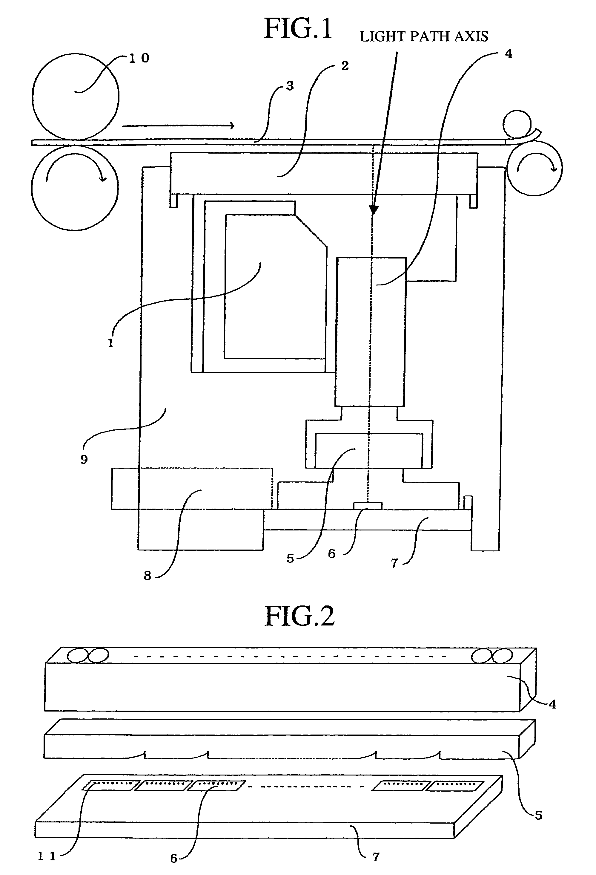
[0036]Hereafter, Embodiment 1 of the present invention will be described. FIG. 1 is a cross sectional view to show a structure of image sensor in accordance with Embodiment 1 of the present invention. In FIG. 1, a reference numeral 1 denotes a light source for applying light to an object to be picked image up (original document, paper money, check, marketable securities and the like), 2 denotes a glass plate for providing a running plane over which the object 3 to be picked image up runs or for protecting and hermetically closing the image sensor, 3 denotes an original document that is the object to be picked image up, 4 denotes a lens (rod lens array) for converging light reflected by the original document 3, 5 denotes a transparent plate for transmitting reflected light, 6 denotes a semiconductor chip composed of an image pickup element and its drive circuit, 7 denotes a sensor substrate on which the semiconductor chip 6 are mounted, 8 denotes a connector for passing and receiving...

embodiment 2

[0045]FIG. 13 shows a transparent plate 51 that is formed to have a protruding portion in place of the cutout portion shown in FIG. 7, as described in Embodiment 1. The protruding portion of this transparent plate 51 will be described with reference to FIG. 14 and FIG. 15 in contrast with FIG. 8 and FIG. 9. If the boundary portion between the medium A and the medium B is inclined right-side down in FIG. 14, the refracted light is bent in the right direction with respect to the incident light. If the boundary portion between the medium A and the medium B is inclined right-side up, the refracted light is bent in the left direction with respect to the incident light. FIG. 15 is a diagram in which the boundaries between the medium A and the medium B in FIG. 15 are overlaid on each other with one on the front side of surface of paper and the other on the back side. In this case, light bent in the right direction of the refracted light relative to the incident vertical light becomes front...

embodiment 3

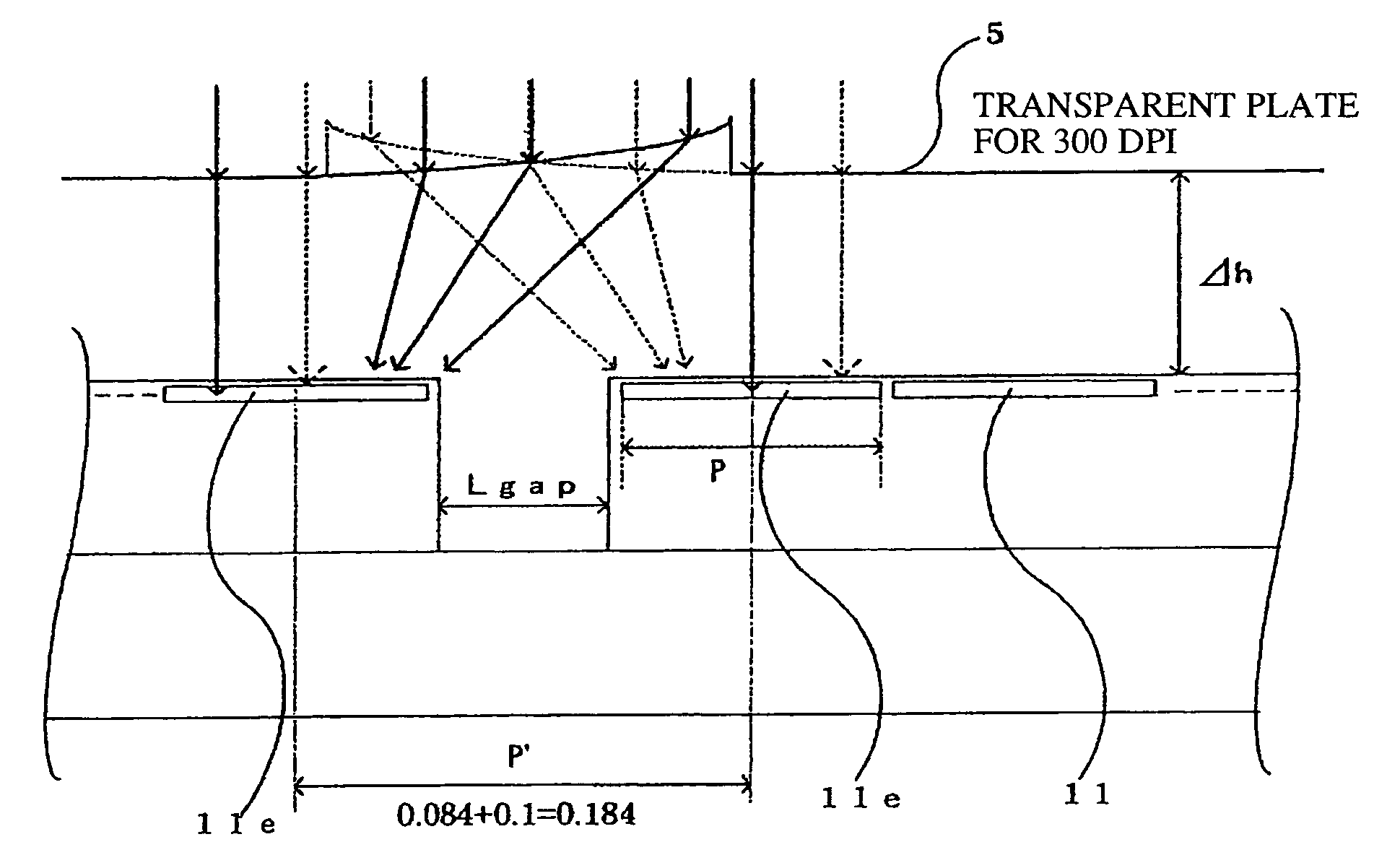
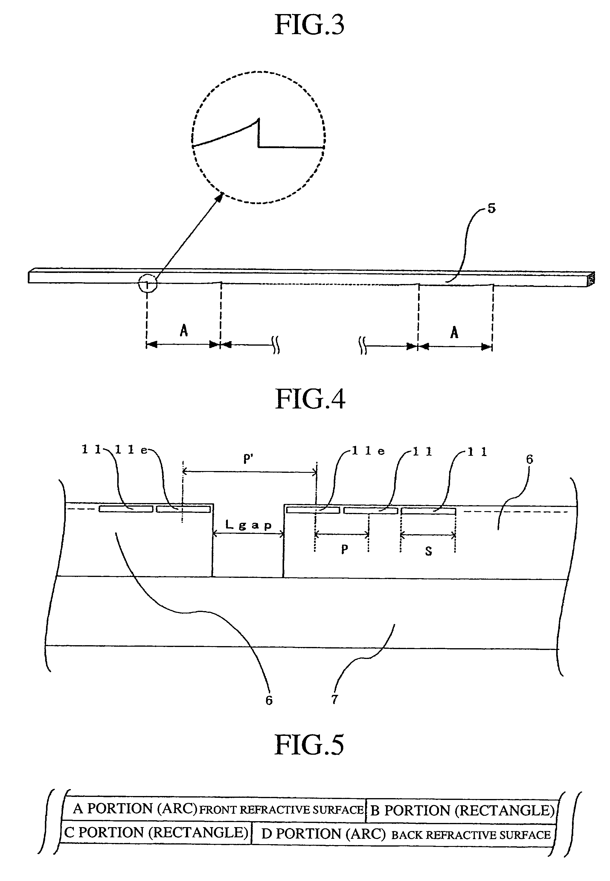
[0046]FIG. 16 is a partial perspective view to show a transparent plate 5 in which the discontinuous region of the transparent plate 5 of image sensor shown in FIG. 7 in Embodiment 1 of the present invention is achieved a light intercepting treatment. In Embodiment 1 and Embodiment 2, the vertical light which incidents on the boundary region between semiconductor chips 6 has been mainly described. However, in actual because there is such reflected effective light from the original document 3 that is slightly inclined with respect to the vertical light and when the transparent plate 5 has the cutout portion of 0.03 mm in height (h) with respect to its thickness (2 mm), a part of the effective light is totally reflected and enters into the other image pickup element 11, thereby to reduce the definition of a read image. In order to prevent this phenomenon, the stepped portion and the inclined portion that are also discontinuous regions located on a plane parallel to the light path axis...


PUM

PropertyMeasurementUnit
heightaaaaaaaaaa
widthaaaaaaaaaa
sizeaaaaaaaaaa

Abstract

An image sensor includes: a sensor substrate on that a large number of semiconductor chips each of which has a plurality of image pickup elements, are linearly arranged to receive the reflected light converged by the lens; and a transparent plate that is interposed between the lens and the sensor substrate, and provides a light path region corresponding to the boundary region between adjacent semiconductor chips with a refractive function, so that the vertical light incident on the boundary region between semiconductor chips 6 is refracted and incident dividedly to the directions of respective image pickup elements.

Description

BACKGROUND OF THE INVENTION[0001]1. Field of the Invention[0002]The present invention relates to an image sensor used for an image input device and in particular, to a contact type image sensor in which a plurality of semiconductor chips are mounted as a photoelectric conversion element.[0003]2. Description of the Related Art[0004]As one structure of an image sensor, an image reading device is disclosed in FIG. 9 in patent document 1, in which a plurality of chips are arranged with prevention for a density difference caused by a pitch error between the chips (at a boundary of the chips) from becoming conspicuous. In the drawing, reference symbols C1 and C2 denote chips (photoelectric conversion elements), Ca and Cb denote chip ends adjacent to each other, La denotes a gap distance between the ends of adjacent chips. Further, a reference symbol r denotes an image pickup element (light receiving element), P denotes a distance between the image pickup elements, P′ denotes a distance be...

Claims


Application Information

Patent Timeline
Patent Type & Authority Patents(United States)
IPC IPC(8): H04N7/173C07C67/52C07C67/54C07C69/82G01S1/02G01S5/02G01S5/06G01S5/12G01S19/27G02B26/10G03B11/00G03B17/02G06F1/16G06F3/00G06F9/46G06F11/00G06F11/10G06F12/10G06F13/00G06F13/12G06F13/36G06F13/362G06F15/00G06F15/16G06F15/173G06K9/00G06K9/62G06K17/00G06K19/00G06T9/00G08C19/16G09C1/00G09G3/02G10L19/00G11B20/10G11B20/14G11B20/18G11B20/22H01L27/00H01L27/146H01Q1/24H01Q21/24H03L7/091H03M13/03H03M13/13H03M13/23H03M13/27H03M13/29H04B1/16H04B1/707H04B7/005H04B7/185H04B7/24H04B7/26H04B14/00H04H60/72H04J3/06H04J13/00H04J13/16H04L1/00H04L1/18H04L7/00H04L9/08H04L9/10H04L9/14H04L9/28H04L9/32H04L12/08H04L12/16H04L12/28H04L12/417H04L12/46H04L12/54H04L25/02H04L25/03H04L25/49H04L25/497H04L27/10H04L27/156H04L27/18H04L47/2416H04L69/40H04M1/00H04M1/66H04M1/715H04M1/724H04M1/72415H04M1/73H04M3/00H04M3/16H04M3/22H04M3/42H04M11/00H04M11/06H04N1/028H04N1/031H04N1/191H04N5/225H04N5/38H04N5/44H04N5/46H04N5/64H04N5/66H04N5/74H04N5/76H04N5/765H04N5/775H04N5/85H04N5/907H04N5/92H04N7/01H04N7/08H04N7/16H04N7/26H04N7/36H04N7/52H04N9/31H04N9/64H04N9/79H04N9/804H04N17/00H04N21/41H04N21/414H04Q3/00H04W4/06H04W4/10H04W4/12H04W4/14H04W4/16H04W8/02H04W8/06H04W8/08H04W8/16H04W8/20H04W8/24H04W8/26H04W24/00H04W24/04H04W24/08H04W24/10H04W28/02H04W28/04H04W28/08H04W28/16H04W28/22H04W36/02H04W36/04H04W36/18H04W36/30H04W40/22H04W48/06H04W48/08H04W48/14H04W48/16H04W52/02H04W52/24H04W56/00H04W60/00H04W64/00H04W68/00H04W68/02H04W72/04H04W72/08H04W72/12H04W72/14H04W74/08H04W76/02H04W76/04H04W76/06H04W80/06H04W84/04H04W84/08H04W84/12H04W84/18H04W88/02H04W88/04H04W88/06H04W88/12H04W88/18H04W92/12
CPCH01L27/14625H04N1/031H04N1/0318H04N1/1934H04N1/1935H04M7/1295H04N1/00957H04N1/32106H04N1/40H04N5/2251H04N5/2257H04N5/4401H04N5/4448H04N5/46H04N5/64H04N5/76H04N7/0112H04N7/163H04N7/17327H04N9/3129H04N9/642H04N9/7925H04N21/2543H04N21/4181H04N21/433H04N21/4623H04N21/47211H04N21/6175H04N21/6187H04N21/6582H04Q3/0025H04Q3/60H04W4/14H04W8/265H04W12/10H04W28/00H04W36/02H04W52/0225H04W52/30H04W56/00H04W64/00H04W68/00H04W74/008H04W74/0816H04W76/022H04W76/064H04W84/08H04W92/02H04L41/06H04L47/10H04L67/1002H04L45/04H04L45/22H04L45/24H04L47/72H04L47/745H04L47/765H04L47/11H04L47/12H04L47/14H04L47/15H04L47/193H04L47/2416H04L47/27H04L47/283H04L47/34H04L47/822H04L47/824H04L49/9094H04L49/90H04J3/0655H04L69/18H04L69/40H04L69/161H04L69/163H04L65/4061H04L41/5009H04L41/5035H04L41/5087H04L43/50H04L65/1043H04L61/2553H04L51/28H04L65/605H04L51/38H04L69/16H04L69/166H04L67/1034G01S1/026G01S5/021G01S5/06G06F12/109G06F1/1626G06F1/1639G06F3/0481G06F21/305G06F21/6209G06F21/74G06F21/88G11B20/10009G11B20/10425H03L7/091H04B7/18582H04B7/2628H04B7/2687H04B10/25754H04J13/0077H04J13/16H04L1/0002H04L1/0015H04L1/0066H04L1/0068H04L1/1685H04L1/1841H04L1/187H04L9/085H04L9/304H04L12/2697H04L12/417H04L12/462H04L12/4641H04L12/5695H04L25/03038H04L25/4902H04L25/4904H04L25/497H04L27/156H04L29/06H04L29/06027H04L29/12471H04L63/126H04L65/1006H04L65/4092H04L65/607H04M1/723H04M1/72533H04M3/007H04M3/16H04M7/0057H04N19/139H04N19/70H04N19/51H04N19/109H04N19/91H04N19/527H04N19/517H04N19/625H04N2201/02493H04N2201/03112H04N2201/03187H04M11/06H04N5/38H04N5/445H04N5/45H04N5/66H04N5/775H04N5/85H04N5/907H04N7/0122H04N9/8042H04W4/10H04W4/12H04W8/245H04W8/26H04W24/00H04W28/04H04W28/18H04W28/26H04W40/00H04W40/02H04W48/08H04W52/0248H04W52/0274H04W72/042H04W72/1252H04W72/1268H04W74/0833H04W76/005H04W76/02H04W76/027H04W76/06H04W80/00H04W84/042H04W84/12H04W88/06H04W88/085H04W88/16H04W92/12G06F2221/2105G06F2221/2115H04L2012/40215H04L2012/40273H04Q2213/1302H04Q2213/13039H04Q2213/1304H04Q2213/13076H04Q2213/13095H04Q2213/13109H04Q2213/13298H04Q2213/13349H04J3/0658H04N2201/0094H04N2201/3274H04N2201/3222Y10S707/99943Y10S370/906Y10S370/907H04L69/14H04L65/1016H04N2201/3212H04L43/0829G11B20/22H04B1/707H04L51/04H04M1/72519H04M3/42221H04N2201/03133H04N2201/03141H04N2201/03145H04L47/70H04W76/18H04W76/45H04W76/30H04W76/34H04W76/12H04W76/10H04N21/426Y02D30/70H04M1/715H04M1/72415H04M1/724H04L43/091H04L51/48H04L51/58H04L65/613H04L65/765H04L65/1104H04L65/70H04L67/1001H04N23/57H04W72/52H04W72/23H04L9/40H04L65/1101H04W8/04
Inventor ENDO, TAKAFUMINOKAMI, YOHEI
Owner MITSUBISHI ELECTRIC CORP
Why Eureka
Try Eureka