System and method for reducing patterning variability in integrated circuit manufacturing through mask layout corrections

a technology of mask layout and patterning, applied in the field of integrated circuit manufacturing, can solve the problems of affecting the patterning accuracy of the image, so as to achieve the effect of superior patterning accuracy and fidelity

Active Publication Date: 2008-01-08
CADENCE DESIGN SYST INC
View PDF39 Cites 151 Cited by
  • Summary
  • Abstract
  • Description
  • Claims
  • Application Information

AI Technical Summary

Benefits of technology

[0020]In another embodiment, a business process is provided for offering a turnkey service to semiconductor manufacturers to carry out compensation of lithography mask data for imperfections in the patterning process and to carry out other RET methodologies. The provider of such turnkey service preferably owns and takes total responsibility for implementing the layout compensation task and provides customers with data for manufacturing masks that will lead to further efficiencies and superior patterning accuracy and fidelity.

Problems solved by technology

But as the CD drops below the illumination wavelength, the image quality degrades rapidly due to diffraction and other effects.
The challenge in patterning at deep sub-wavelength feature sizes stems from the fact that image patterns as printed on the wafer get distorted from the original intended patterns, as illustrated in FIG. 4.
The difficulty with this approach is that it is iterative in nature and takes long computation times.
While these prior art techniques improve the patterning accuracy and CD uniformity, CD variations today remain intolerably high, both within an IC chip and across a stepper field, and will become increasingly more problematic at 0.13 μm and finer feature sizes.
As the lithographic process advances from 248-nm to 193-nm stepper technologies and beyond, ACLV / AFLV problems will continue to get worse.
One of the reasons the prior art techniques still leave a sizable portion of the image distortions uncorrected is that they assume that these distortions are fixed across the entire chip as well as the stepper field.
Furthermore, they are designed for general applicability and do not take into account the specific tools- or process-induced aberrations and their unique variability signatures.
In MOPC, the modeling does not adequately factor the within-field variations.

Method used


Image

  • System and method for reducing patterning variability in integrated circuit manufacturing through mask layout corrections
  • System and method for reducing patterning variability in integrated circuit manufacturing through mask layout corrections
  • System and method for reducing patterning variability in integrated circuit manufacturing through mask layout corrections

Examples


Embodiment Construction

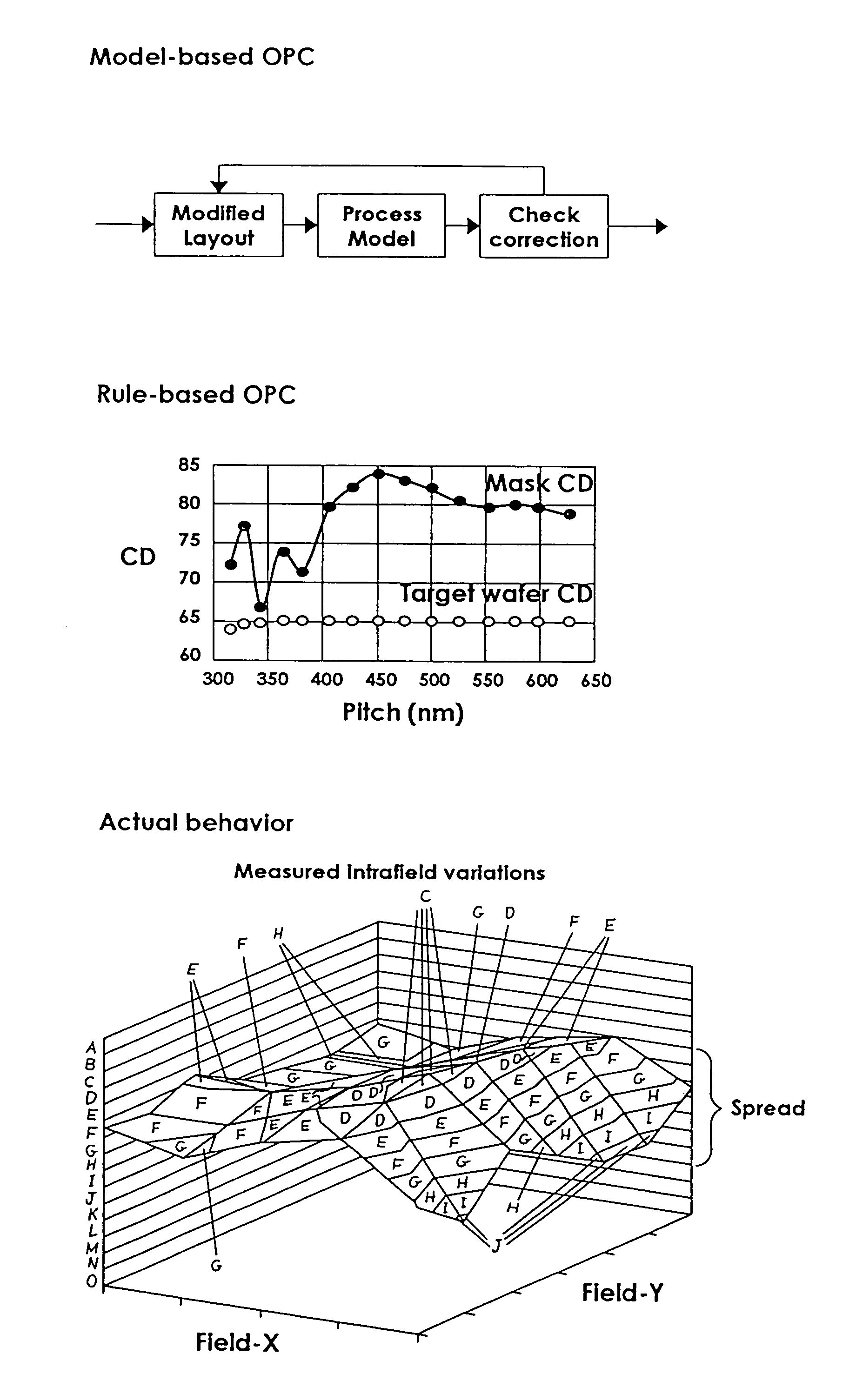
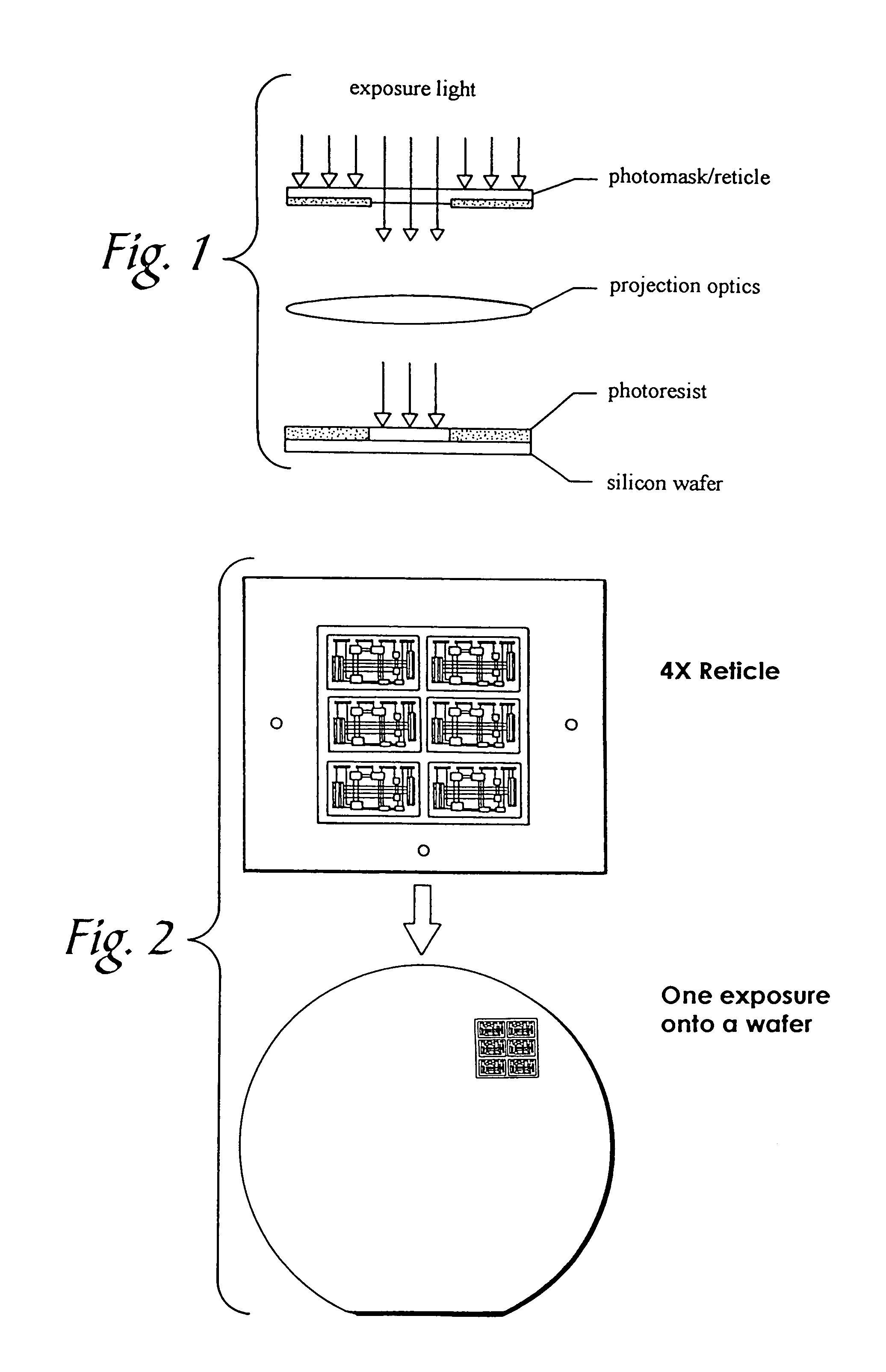
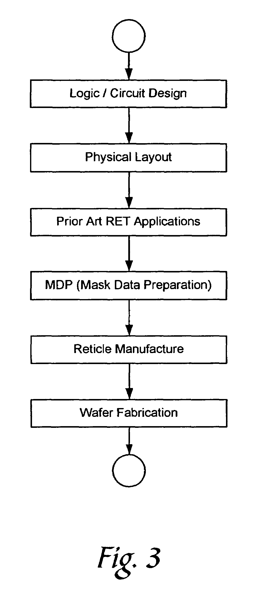
[0038]Referring now to FIG. 7, there is shown the level of layout compensations as provided by the present invention. Starting from a rectangular reticle field, a set of correction zones is first mapped onto the field. The correction zones follow the natural tool / process-induced regions of aberrations. For practical purposes, these complex aberration regions may be reduced to a set of regions with more regular geometrical shapes, such as a grid of rectangular partitions of the same or varying sizes that are sufficiently small that within each such grid, the properties of the aberrations may be described in simpler mathematical terms. Each such partitioned space is called a Compensation Zone, where a zone is intended as the unit of application of the corrections. In the description here, for the sake of simplicity, a rectangular grid of compensation zones is assumed. As the patterning is done on an entire reticle field basis, zoning allows the peculiar local variability characteristi...


PUM


Abstract

The present invention provides a system and method of modifying the mask layout shapes of an integrated circuit layout design to compensate for reticle field location-specific systematic CD variations resulting from mask writing process variations, lens imperfections in lithographic patterning, and photoresist process variations. Called PLC (Process-optimized Layout Compensation), each set of compensation rules according to the present invention is specifically tailored for a particular mask-writer-patterning-tools-and-resist-process combination, and are performed on a reticle-wide basis. Furthermore, for each geometric shape in the mask layout, the amount of modification is determined based on a categorization of the type of the shape, the specific location in the reticle field the particular shape falls in, its context (i.e., surrounding patterns, orientation, etc.), as well as certain photoresist parameters to be used in the patterning process.

Description

CROSS-REFERENCE TO RELATED APPLICATION[0001]This application claims the benefit of U.S. provisional application No. 60 / 480,286, filed Jun. 19, 2003, which is hereby incorporated by reference.BACKGROUND OF THE INVENTION[0002]1. Field of the Invention[0003]The present invention relates in general to integrated circuit (IC) manufacture, and more particularly to improving patterning accuracy and minimization of line-width variations in the optical patterning process used to print a pattern on a photoresist layer on a semiconductor wafer.[0004]2. Description of Related Art[0005]Manufacture of integrated circuit devices involves repeated sequences of the steps of deposition, photolithographic patterning, and etching. During deposition, a layer of conductive or insulating material is deposited on the surface of a silicon wafer. This material is then coated with a photosensitive resist. During the step of photolithographic patterning, which includes a set of optical and chemical processes, ...

Claims


Application Information

Patent Timeline
Patent Type & Authority Patents(United States)
IPC IPC(8): G06F17/50
CPCG03F1/144G03F1/36G03F7/70441G03F1/76G03F1/68G03F1/70
Inventor PRASAD, ROY V.HORNG, CHI-SONGRAMANUJAM, RAM S.
Owner CADENCE DESIGN SYST INC
Why Eureka
Try Eureka