Lithography method and system with adjustable reflector

a technology of reflectors and lithography methods, applied in the field of lithography methods, can solve the problems of optical systems no longer being able to achieve the required resolution, and the resolution requirements have increased

Active Publication Date: 2005-12-20
GLOBALFOUNDRIES US INC
View PDF9 Cites 97 Cited by
  • Summary
  • Abstract
  • Description
  • Claims
  • Application Information

AI Technical Summary

Problems solved by technology

However, with decreasing feature sizes, resolution requirements have increased to the point that optical systems may no longer be able to achieve the required resolution, due to limits inherently related to the wavelengths of optical light employed in such systems.

Method used


Image

  • Lithography method and system with adjustable reflector
  • Lithography method and system with adjustable reflector
  • Lithography method and system with adjustable reflector

Examples


Embodiment Construction

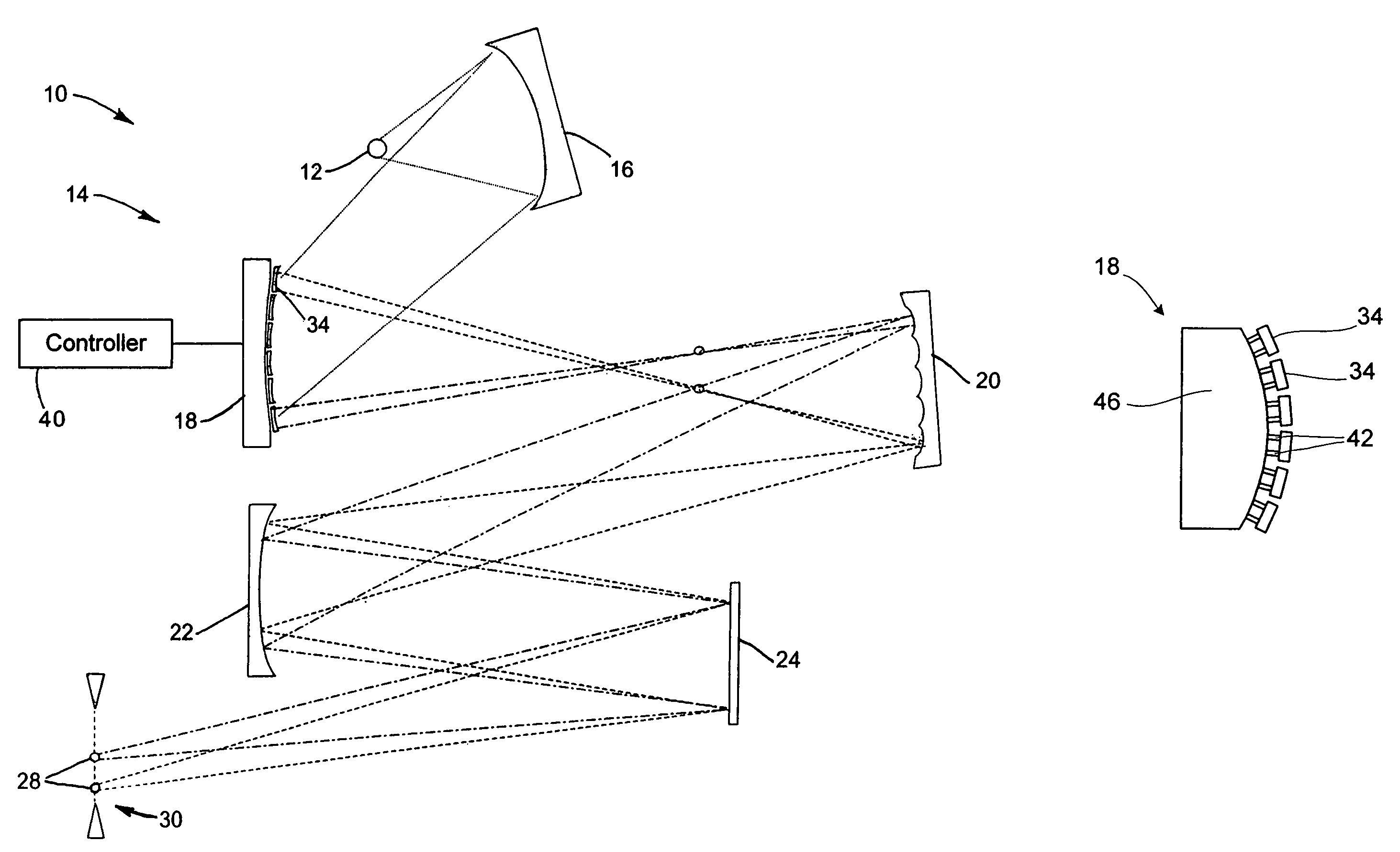
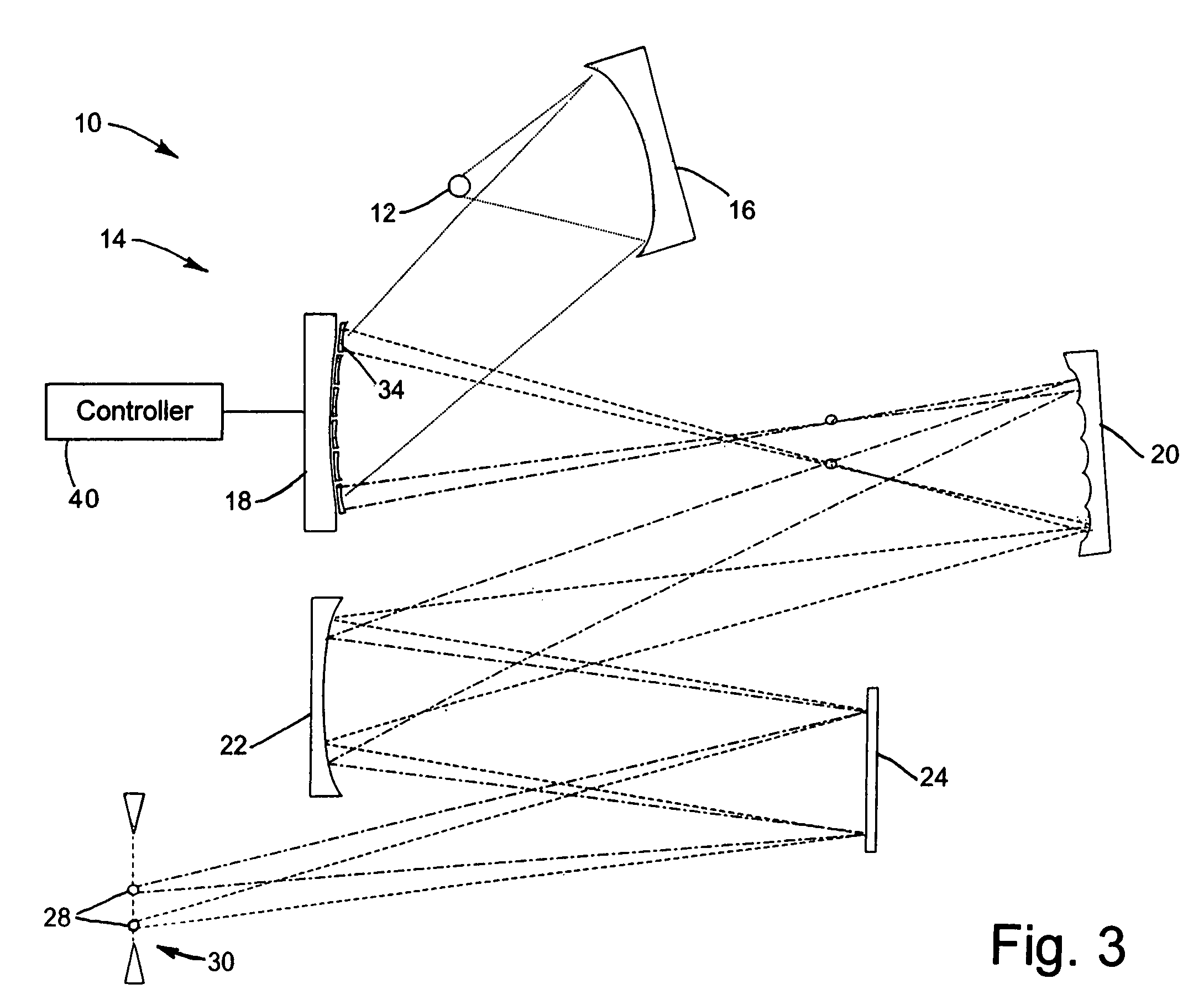
[0029]A method of reflective lithography includes placing an adjustable (configurable) multi-faceted mirror in a condenser that collects and redirects light from a source to a reticle, an imaging system, and finally a target to be patterned. The adjustable multi-faceted mirror has a plurality of separately adjustable mirror elements or facets. The orientation of the mirror elements may be adjusted to adjust the characteristics of the light reaching a reflective reticle in order to achieve certain imaging characteristics at the resist layer that is being exposed. For example, coherence, shape of the illumination at the pupil of the imaging system, and / or configuration of the light output may be changed. The method and a corresponding system may be employed in extreme ultraviolet light (EUVL) lithography.

[0030]FIG. 3 shows a portion of a lithography system 10. The lithography system 10 includes a light (radiation) source 12. The light from the light source 12 is directed by a condense...


PUM

PropertyMeasurementUnit
wavelengthaaaaaaaaaa
wavelengthsaaaaaaaaaa

Abstract

A method of reflective lithography includes placing an adjustable (configurable) multi-faceted mirror in a condenser that collects and redirects light from a source to a reticle, an imaging system, and finally a target to be patterned. The adjustable multi-faceted mirror has a plurality of separately adjustable mirror elements or facets. The orientation of the mirror elements may be adjusted to adjust the characteristics of the light reaching a reflective reticle in order to achieve certain imaging characteristics at the resist layer that is being exposed. For example, coherence, shape of the illumination at the pupil of the imaging system, and / or configuration of the light output may be changed. The method and a corresponding system may be employed in extreme ultraviolet light (EUVL) lithography.

Description

BACKGROUND OF THE INVENTION[0001]1. Field of the Invention[0002]The invention relates generally to lithography methods for producing semiconductor devices.[0003]2. Background of the Related Art[0004]In the semiconductor field, there has been and continues to be a trend toward smaller devices and higher device densities. This trend shows no signs of abating in the future. Higher densities require the reducing of device sizes and / or distance between devices on semiconductor wafers. In addition, the overall size and / or spacing of interconnects between devices may also need to be reduced.[0005]The trend towards higher device densities leads to a requirement for increased resolution in lithographic processes, such as photolithographic processes. Generally speaking, lithography involves any of a variety of processes for transferring patterns between various types of media. With particular regard to semiconductor fabrication processes, silicon or other semiconductor material may be coated ...

Claims


Application Information

Patent Timeline
Patent Type & Authority Patents(United States)
IPC IPC(8): G02B26/08G03B27/42G03F7/20
CPCG02B26/0858G03F7/70116G03F7/70583
Inventor LAFONTAINE, BRUNO M.
Owner GLOBALFOUNDRIES US INC
Why Eureka
Try Eureka