

Superconducting low inductance qubit
a low-inductance, superconducting technology, applied in the field of quantum computing, can solve the problems of limiting the usefulness of the device, difficult to expand the expansion of such systems to a commercially useful number of qubits, and inherently difficult simulation of quantum systems
- Summary
- Abstract
- Description
- Claims
- Application Information
AI Technical Summary
Benefits of technology
Problems solved by technology
Method used
Image

Examples
Embodiment Construction
Terminology
[0041]The following terms are used herein with meanings that would be familiar to one of ordinary skill in the art of quantum computing, but a brief explanation is presented for the purpose of clarity. The reader is also referred to standard works of reference in the field, such as: Quantum Computation and Quantum Information, M. A. Nielsen, and I. L. Chuang, Cambridge University Press, (2000); and Scalable Quantum Computers—Paving the Way to Realization, S. L. Braunstein and H.-K. Lo (eds), Wiley-VCH, (2001). A standard work on superconductivity is: J. R. Schrieffer and M. Tinkham, “Superconductivity”, Reviews of Modern Physics, 71(2), S313-S317, (1999).
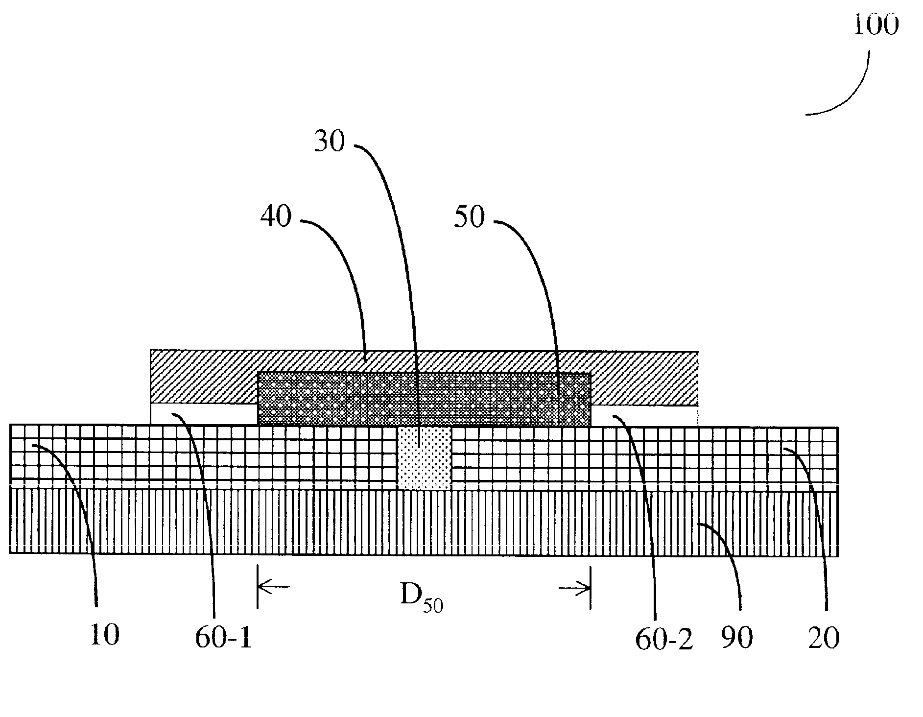
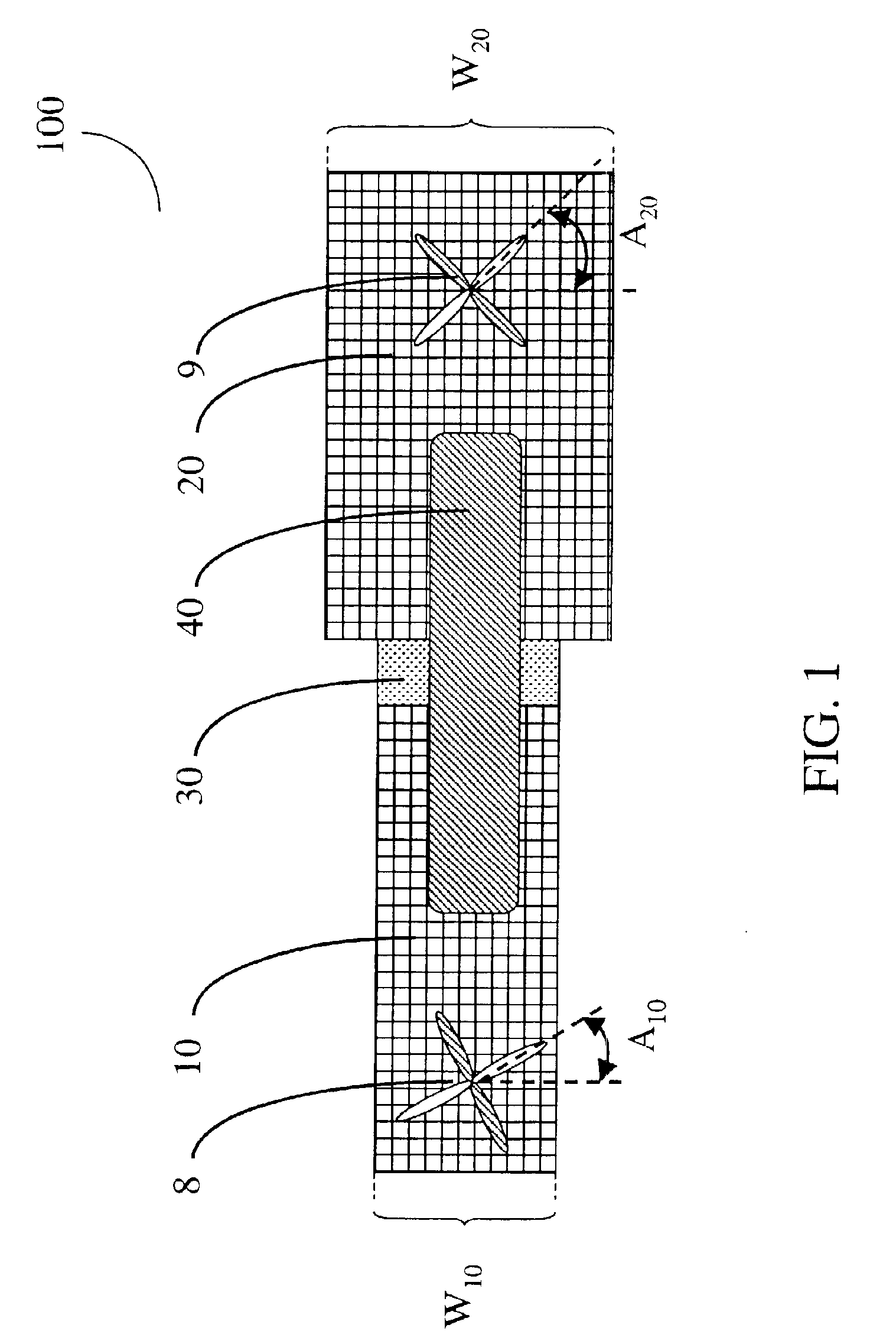
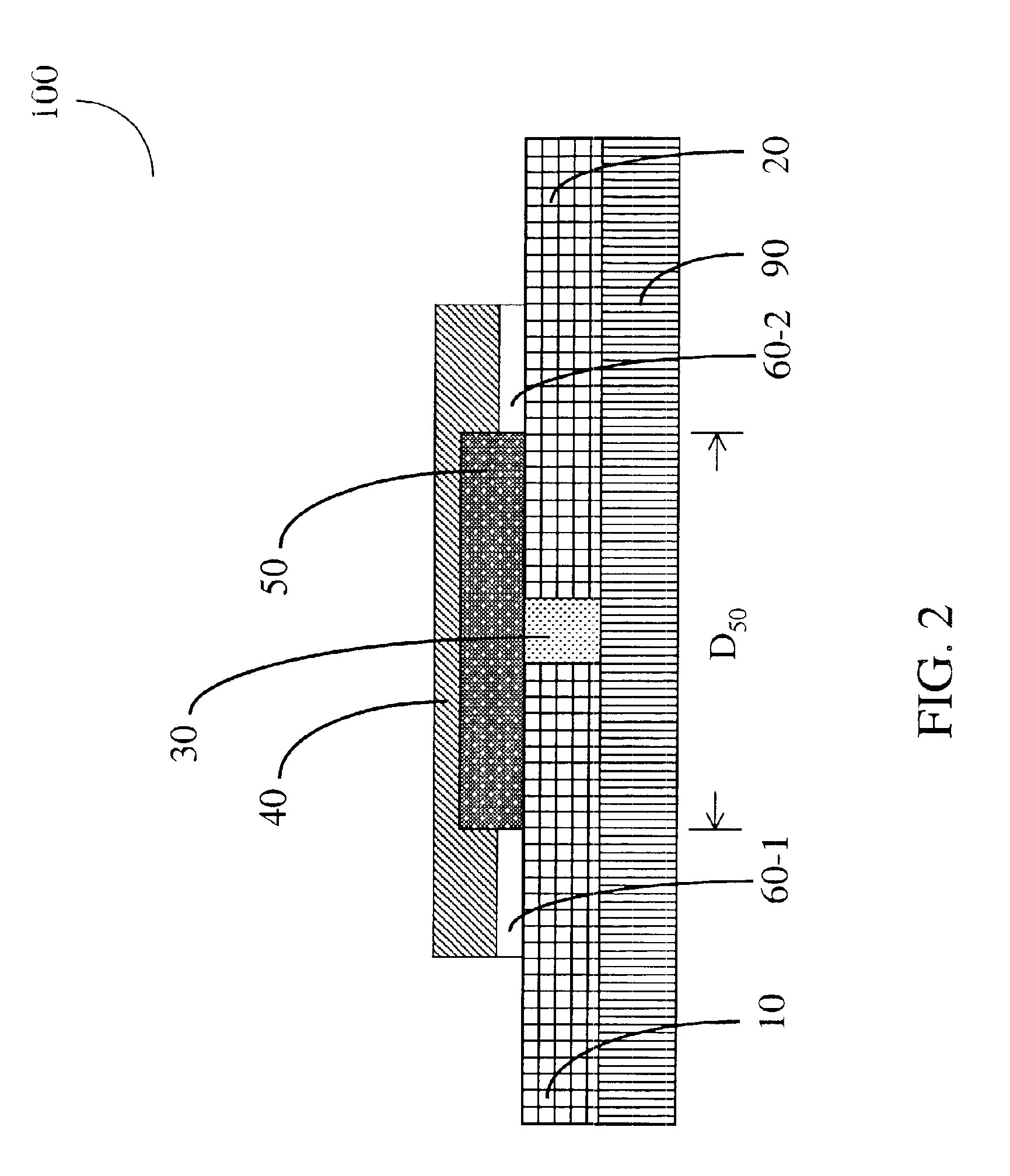
[0042]Superconductor, or superconducting material: A material whose electrical resistance disappears completely under certain conditions. Most superconducting materials only superconduct over narrow ranges of temperature, current, pressure, and magnetic field. Theoretically, a loop of superconducting material is able to s...
PUM
 Abstract
Description
Claims
Application Information