
Amplitude conversion circuit for converting signal amplitude

Active Publication Date: 2005-12-27
TRIVALE TECH LLC
View PDF18 Cites 39 Cited by
  • Summary
  • Abstract
  • Description
  • Claims
  • Application Information

AI Technical Summary

Benefits of technology

[0015]One object of the present invention is to provide an amplitude conversion circuit and a semiconductor device using the amplitude conversi

Problems solved by technology

However, there is a considerable difference in the threshold voltage between low-temperature polysilicon TFTs included in the liquid crystal display, which makes it difficult to set the threshold voltage of the TFTs at 3 V or less.
However, the cost of level shifter 72 thus provided adds to the system cost, resulting in increase of the system cost.

Method used


Image

  • Amplitude conversion circuit for converting signal amplitude
  • Amplitude conversion circuit for converting signal amplitude
  • Amplitude conversion circuit for converting signal amplitude

Examples


Embodiment Construction

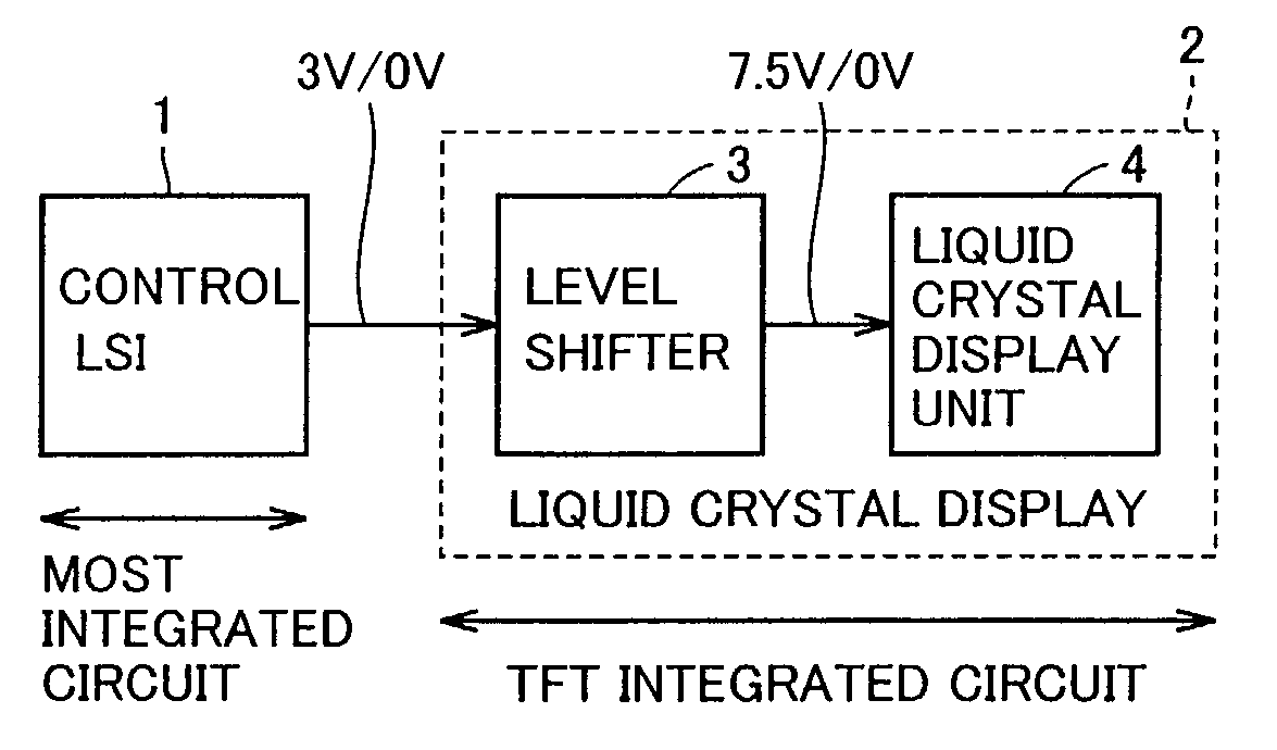
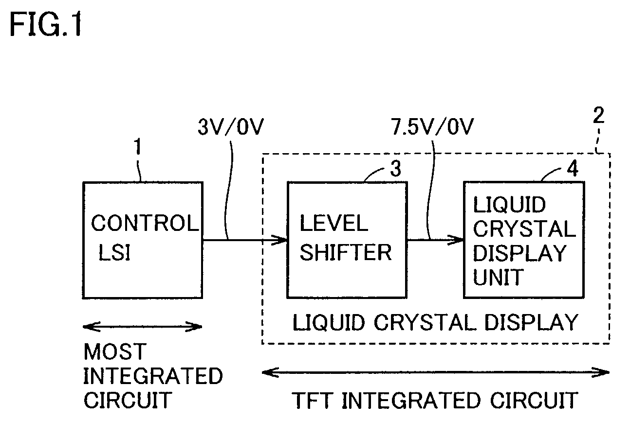
[0024]FIG. 1 is a block diagram showing a configuration of a part of a cellular phone that is involved in image display according to one embodiment of the present invention.

[0025]Referring to FIG. 1, the cellular phone includes a control LSI 1 which is a MOST integrated circuit and a liquid crystal display 2 which is a TFT integrated circuit. Liquid crystal display 2 includes a level shifter 3 and a liquid crystal display unit 4.

[0026]Control LSI 1 generates a control signal for liquid crystal display 2. The control signal has its H level of 3 V and its L level of 0 V. Although a large number of control signals are actually generated, it is assumed here for convenience of description that one control signal is generated. Level shifter 3 changes the logic level of the control signal from control LSI 1 to generate an internal control signal. The internal control signal has its H level of 7.5 V and its L level of 0 V. Liquid crystal display unit 4 presents an image according to the int...


PUM


Abstract

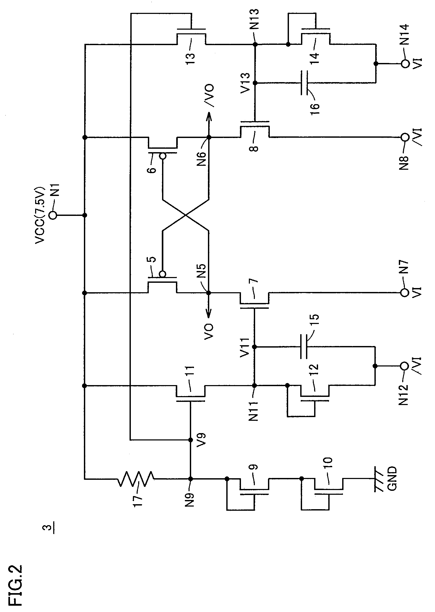
A level shifter includes first and second P-type TFTs for latching a level of first and second output nodes, first and second N-type TFTs for setting the level of the first and second output nodes, and a drive circuit. The drive circuit includes third to eighth N-type TFTs providing, in response to rising and falling edges of an input signal, a voltage higher than a threshold voltage of the first and second N-type TFTs, between the gate and source of the first and second N-type TFTs, and includes first and second capacitors and a resistor element. Accordingly, even if an amplitude voltage of an input signal is smaller than the threshold voltage of the first and second N-type TFTs, the level shifter operates normally.

Description

RELATED APPLICATIONS[0001]The application is a Continuation-In-Part of U.S. patent application Ser. No. 10 / 253,812, filed Sep. 25, 2002 now abandoned, which is incorporated herein by reference.BACKGROUND OF THE INVENTION[0002]1. Field of the Invention[0003]The present invention relates to amplitude conversion circuits. In particular, the present invention relates to an amplitude conversion circuit for changing an amplitude of a signal.[0004]2. Description of the Background Art[0005]FIG. 27 is a block diagram showing a configuration of a part of a conventional cellular phone that is involved in image display.[0006]Referring to FIG. 27, the cellular phone includes a control LSI 71 which is a MOST (MOS transistor) integrated circuit, a level shifter 72 which is also a MOST integrated circuit, and a liquid crystal display 73 which is a TFT (thin-film transistor) integrated circuit.[0007]Control LSI 71 generates a control signal for liquid crystal display 73. The control signal has an H ...

Claims


Application Information

Patent Timeline
IPC IPC(8): G09G3/36H03K3/356H03K19/0175H03K19/0185H03L5/00
CPCH03K3/356113H03K3/356147H03K19/018507G09G3/3648G09G2310/0289
Inventor TOBITA, YOUICHI
Owner TRIVALE TECH LLC
Learn More