Method of manufacturing image display device
- Summary
- Abstract
- Description
- Claims
- Application Information
AI Technical Summary
Benefits of technology
Problems solved by technology
Method used
Image
Examples
Embodiment Construction
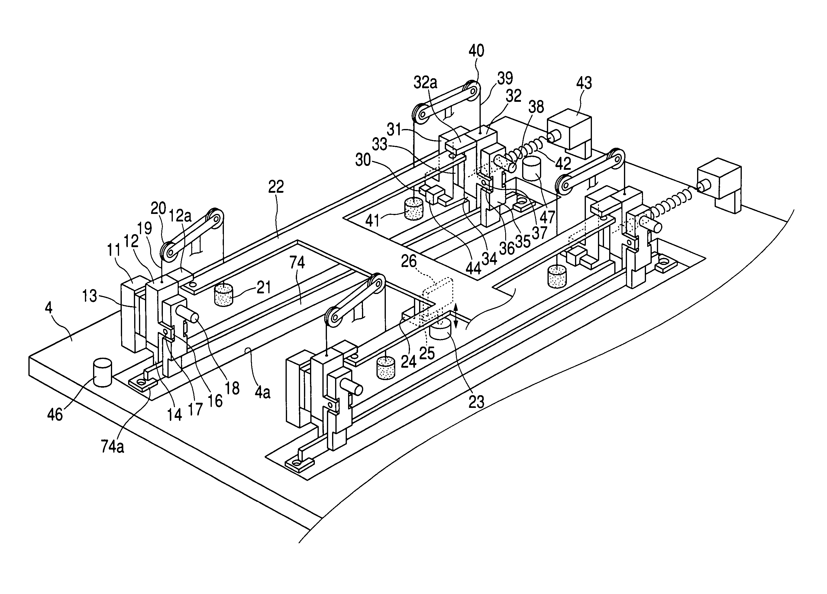
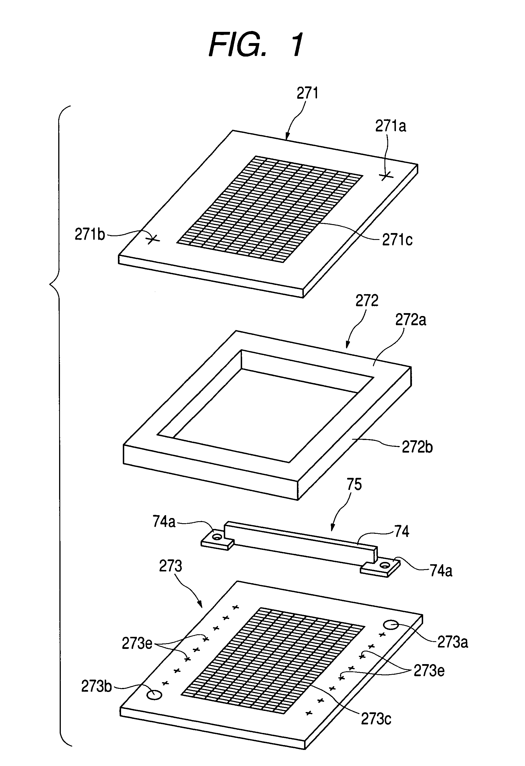
[0031]An embodiment of a method of manufacturing an image display device in accordance with the present invention is described below with reference to FIGS. 1 to 16.
[0032]First, an image display device to be manufactured by the manufacture method according to this embodiment is outlined. This image display device has, as a pair of substrates (plates) facing each other, a rear plate on which electron-emitting devices form a matrix pattern and a face plate on which phosphors are formed at positions opposing the electron-emitting devices on the rear plate. The electron-emitting devices on the rear plate project electron beams at the opposing phosphors on the face plate, thereby causing the phosphors to emit light. The space between the plates in this image display device is in a vacuum and therefore spacers (long spacers) are provided to support the atmospheric pressure applied to the plates.
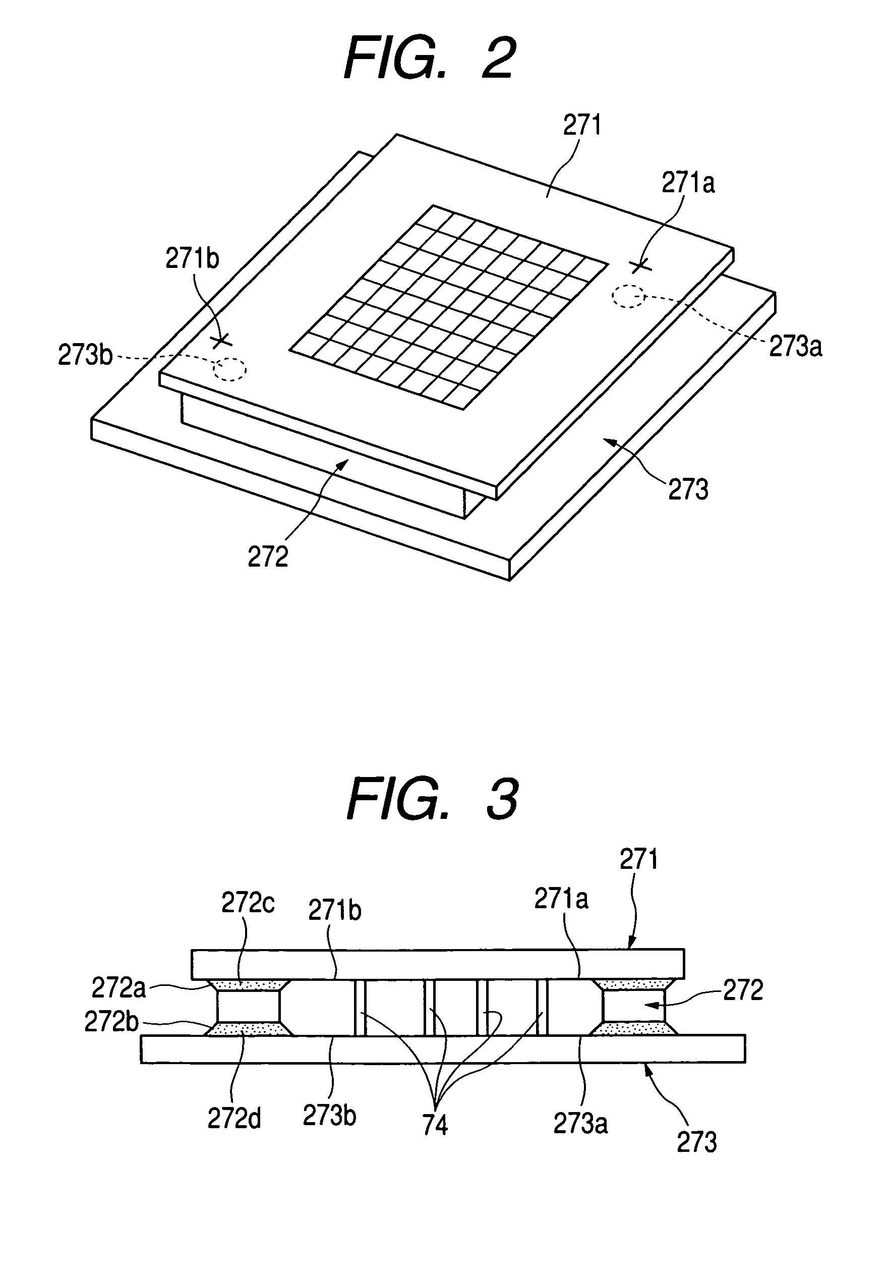
[0033]FIG. 1 is an exploded view of the image display device. FIG. 2 is a perspective view of t...
PUM
 Abstract
Description
Claims
Application Information


