Magnetic memory element utilizing spin transfer switching and storing multiple bits

a memory element and spin transfer technology, applied in the field of magnetic systems, can solve the problems of increasing the area and complexity of the stack, increasing the number of hosts, and increasing the number of cross-talk and power consumption, so as to reduce the height of the stack

Inactive Publication Date: 2006-01-10
SAMSUNG SEMICON
View PDF10 Cites 334 Cited by
  • Summary
  • Abstract
  • Description
  • Claims
  • Application Information

AI Technical Summary

Benefits of technology

[0011]According to the system and method disclosed herein, the present invention provides a magnetic element capable of storing multiple bits and being written using spin transfer switching, which is more localized than the field switching mechanism.

Problems solved by technology

This large current can cause a host of problems in the conventional magnetic memories using the conventional magnetic elements 10 or 20.
For example, cross talk and power consumption would increase.
In addition, the driving circuits required to drive the current that generates the switching field at the desired conventional memory element 10 or 20 would also increase in area and complexity.
This upper limit on the write current amplitude can lead to reliability issues because the cells that are harder to switch than others (due to fabrication and material nonuniformity) will fail to write consistently.

Method used


Image

  • Magnetic memory element utilizing spin transfer switching and storing multiple bits
  • Magnetic memory element utilizing spin transfer switching and storing multiple bits
  • Magnetic memory element utilizing spin transfer switching and storing multiple bits

Examples


second embodiment

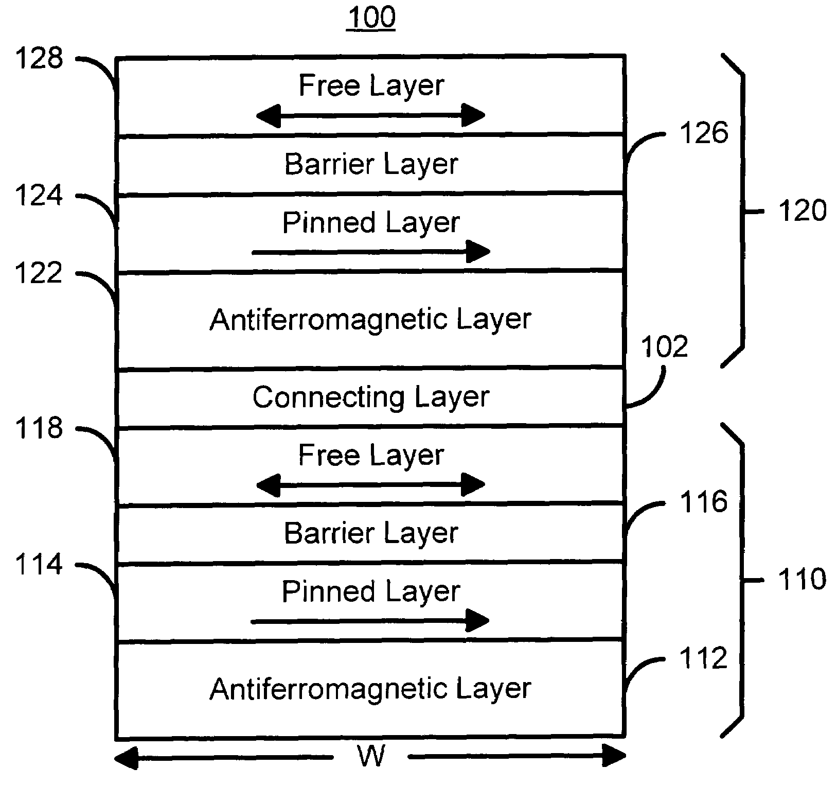
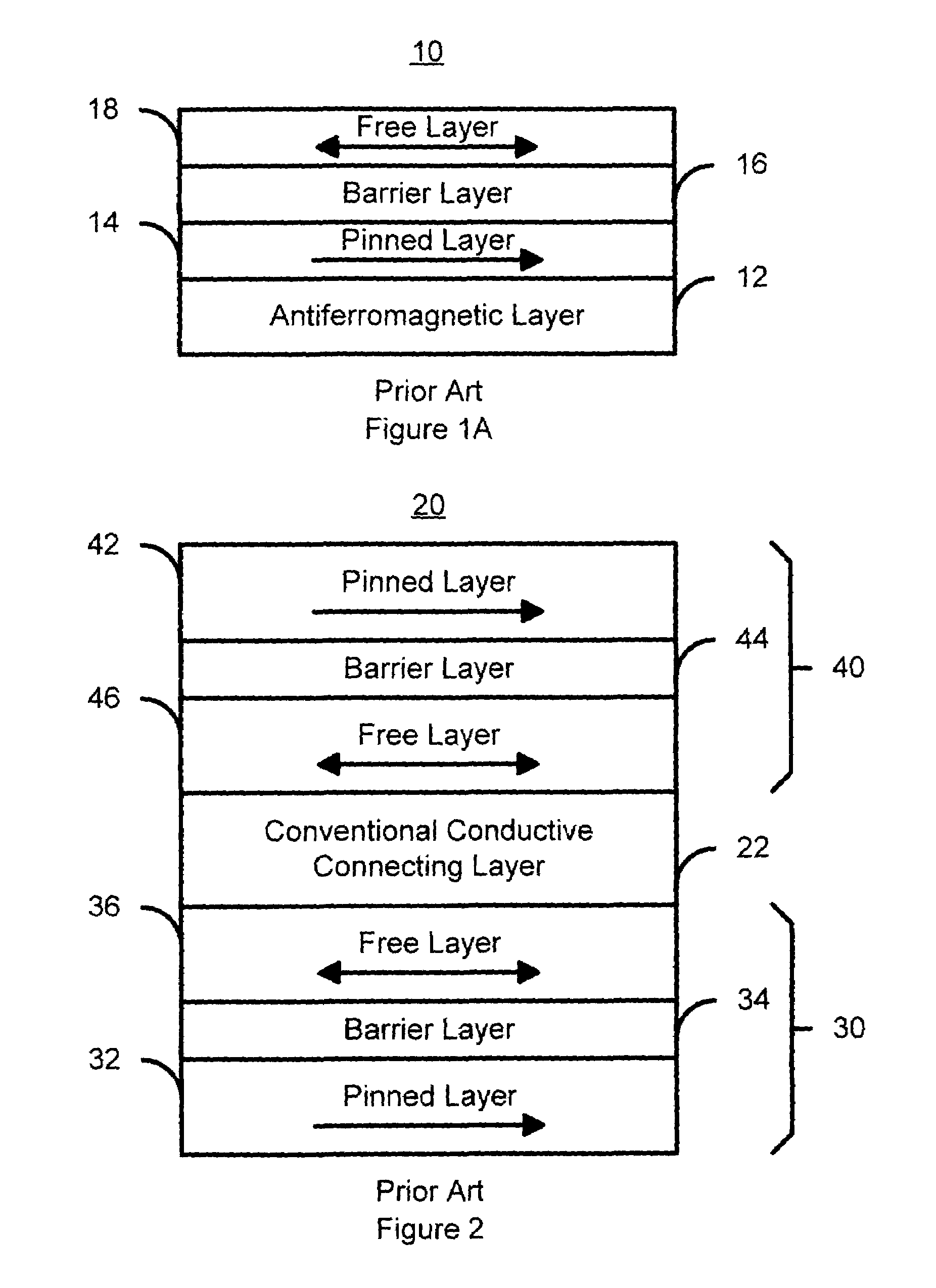
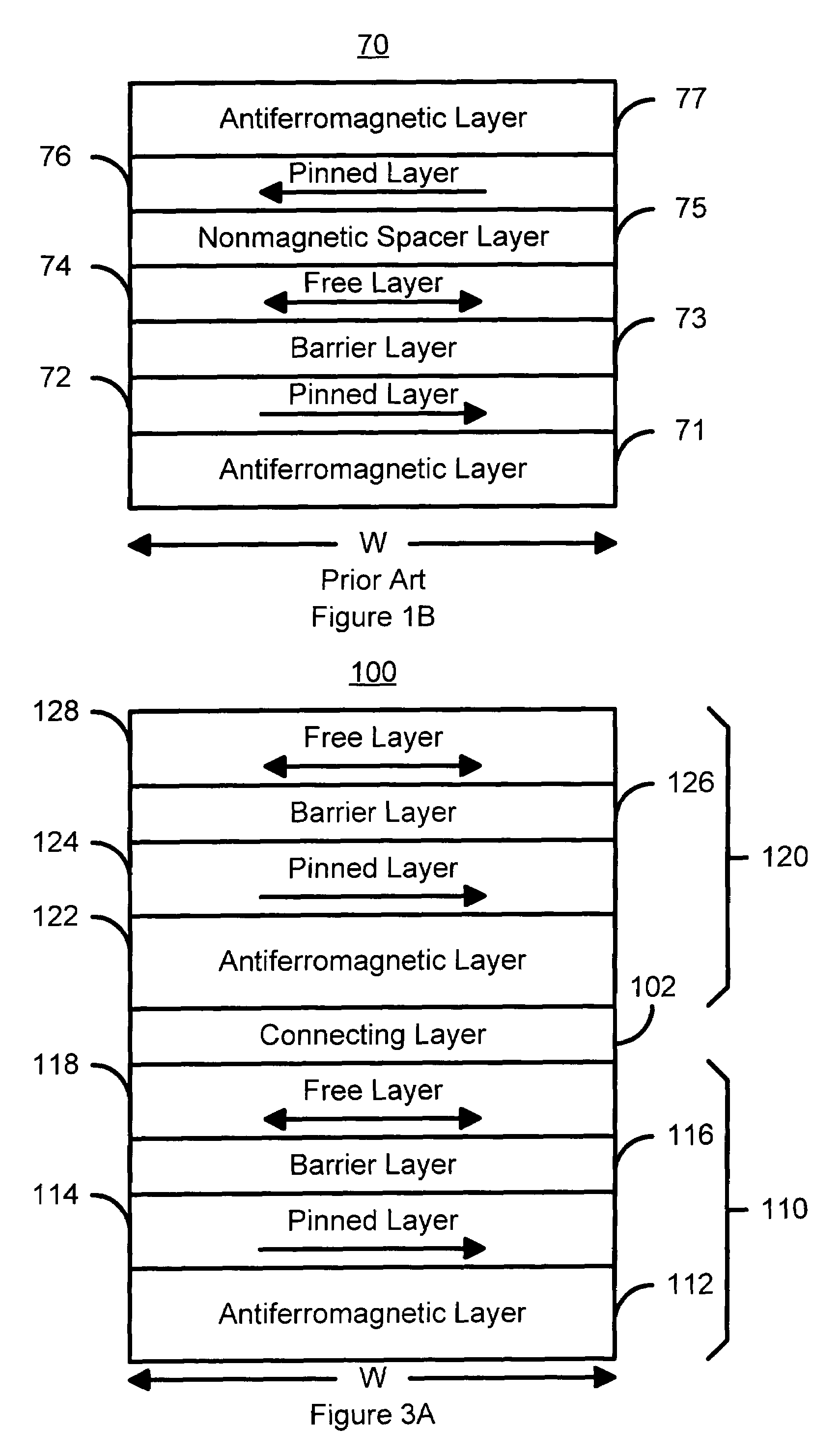
[0052]FIG. 4A is a diagram of a magnetic element 100′ in accordance with the present invention capable of storing multiple bits and utilizing the spin transfer phenomenon for writing. Many of the components of the magnetic element 100′ are analogous to those of the magnetic element 100 depicted in FIG. 3A. Consequently, these components are labeled similarly. For example, the magnetic element 100′ includes spin tunneling junctions 110′ and 120′. However, the connecting layer 102 has been replaced by shared AFM layer 102′. In addition, the AFM layers 112 and 122 have been omitted. Instead, the single shared AFM layer 102′ functions as both a connecting layer (similar to the connecting layer 102) and a layer used to pin the magnetizations of the pinned layers 114′ and 124′ (similar to the AFM layers 102 and 112). Alternatively, to further reduce stack's height, the pinned layers 114′ and 124′ and pinning AFM layer 102′ can be replaced by an antiferromagnetically coupled hard magnetic ...

third embodiment

[0054]FIG. 5A is a diagram of a magnetic element 200 in accordance with the present invention capable of storing multiple bits, utilizing the spin transfer phenomenon for writing, and utilizing a dual spin tunnel / valve structure. The magnetic element 200 thus includes dual spin tunnel / valve structures 210 and 230 separated by a connecting layer 202. The dual spin tunnel / valve structure 210 includes a pinned layer 214, a nonmagnetic layer 216, a free layer 218, a barrier layer 220, and a pinned layer 222. The dual spin tunnel / valve structure 210 also preferably includes AFM layers 212 and 224 used to pin the magnetizations of the pinned layers 214 and 222, respectively. The dual spin tunnel / valve structure 230 includes a pinned layer 234, a nonmagnetic layer 236, a free layer 238, a barrier layer 240, and a pinned layer 242. The dual spin tunnel / valve structure 230 also preferably includes AFM layers 232 and 244 used to pin the magnetizations of the pinned layers 234 and 242, respect...

fourth embodiment

[0060]FIG. 5B is a diagram of a magnetic element 200′ in accordance with the present invention capable of storing multiple bits, utilizing the spin transfer phenomenon for writing, and utilizing a dual spin tunnel / valve structure. The magnetic element 200′ is analogous to the magnetic element 200. Consequently, many of the components are labeled similarly. However, the positions of the nonmagnetic spacer layers 236′ and 216′ and barrier layers 220′ and 240′, respectively, have been reversed. However, the magnetic element 200′ functions in substantially the same manner as the magnetic element 200. Consequently, the dual spin tunnel / valve structure 210′ and 230′ can be written by driving a current through the magnetic element 200′ and exploiting spin transfer as described above. Thus, the magnetic element 200′ has many of the same advantages as the magnetic element 200.


PUM

PropertyMeasurementUnit
depthaaaaaaaaaa
thicknessaaaaaaaaaa
currentaaaaaaaaaa

Abstract

A method and system for providing a magnetic element capable of storing multiple bits is disclosed. The method and system include providing first pinned layer, a first nonmagnetic layer, a first free layer, a connecting layer, a second pinned layer, a second nonmagetic layer and a second free layer. The first pinned layer is ferromagnetic and has a first pinned layer magnetization pinned in a first direction. The first nonmagnetic layer resides between the first pinned layer and the first free layer. The first free layer being ferromagnetic and has a first free layer magnetization. The second pinned layer is ferromagnetic and has a second pinned layer magnetization pinned in a second direction. The connecting layer resides between the second pinned layer and the first free layer. The second nonmagnetic layer resides between the second pinned layer and the second free layer. The second free layer being ferromagnetic and having a second free layer magnetization. The magnetic element is configured to allow the first free layer magnetization and the second free layer magnetization to change direction due to spin transfer when a write current is passed through the magnetic element.

Description

FIELD OF THE INVENTION[0001]The present invention relates to magnetic systems, and more particularly to a method and system for providing a reduced-sized magnetic element, including but not limited to a magnetic element that employs a spin transfer effect in switching and that can be used in a magnetic memory such as magnetic random access memory (“MRAM”).BACKGROUND OF THE INVENTION[0002]Various types of magnetic technology utilize magnetic elements for storing or reading data. For example, in conventional MRAM technology, the conventional magnetic element used is a spin tunneling junction. FIG. 1A depicts one such conventional magnetic element 10, which is a spin tunneling junction 10. The conventional spin tunneling junction 10 includes an antiferromagnetic (AFM) layer 12, a pinned layer 14, a barrier layer 16, and a free layer 18. The conventional pinned layer 14 is ferromagnetic and has a magnetization that is typically pinned by the AFM layer 12. As used herein, the term “ferro...

Claims


Application Information

Patent Timeline
Patent Type & Authority Patents(United States)
IPC IPC(8): G11C11/15G11C11/16H01F10/32H01L43/08
CPCB82Y25/00G11C11/16H01L43/08H01F10/3263G11C11/5607H10N50/10G11C11/15H10B61/00
Inventor NGUYEN, PAUL P.HUAI, YIMING
Owner SAMSUNG SEMICON
Why Eureka
Try Eureka