System-on-a-Chip structure having a multiple channel bus bridge

a technology of system-on-chip and bus bridge, which is applied in the direction of instruments, electric digital data processing, etc., can solve the problems of requiring several system clock cycles of latency, affecting the performance of bus system hierarchies, and achieving poor performance of conventional component-based system-on-a-chip communication architectures

Inactive Publication Date: 2006-01-10
GLOBALFOUNDRIES US INC
View PDF8 Cites 33 Cited by
  • Summary
  • Abstract
  • Description
  • Claims
  • Application Information

AI Technical Summary

Problems solved by technology

Conventional component-based System-on-a-Chip (SoC) communication architectures achieve poor performance.
This is primarily due to the blocking nature of their on-chip communication structures associated with handshake protocols, interconnecting processors and their peripheral Intellectual Property (IP) blocks, which induces latencies that degrade performances of bus system...

Method used


Image

  • System-on-a-Chip structure having a multiple channel bus bridge
  • System-on-a-Chip structure having a multiple channel bus bridge
  • System-on-a-Chip structure having a multiple channel bus bridge

Examples


Embodiment Construction

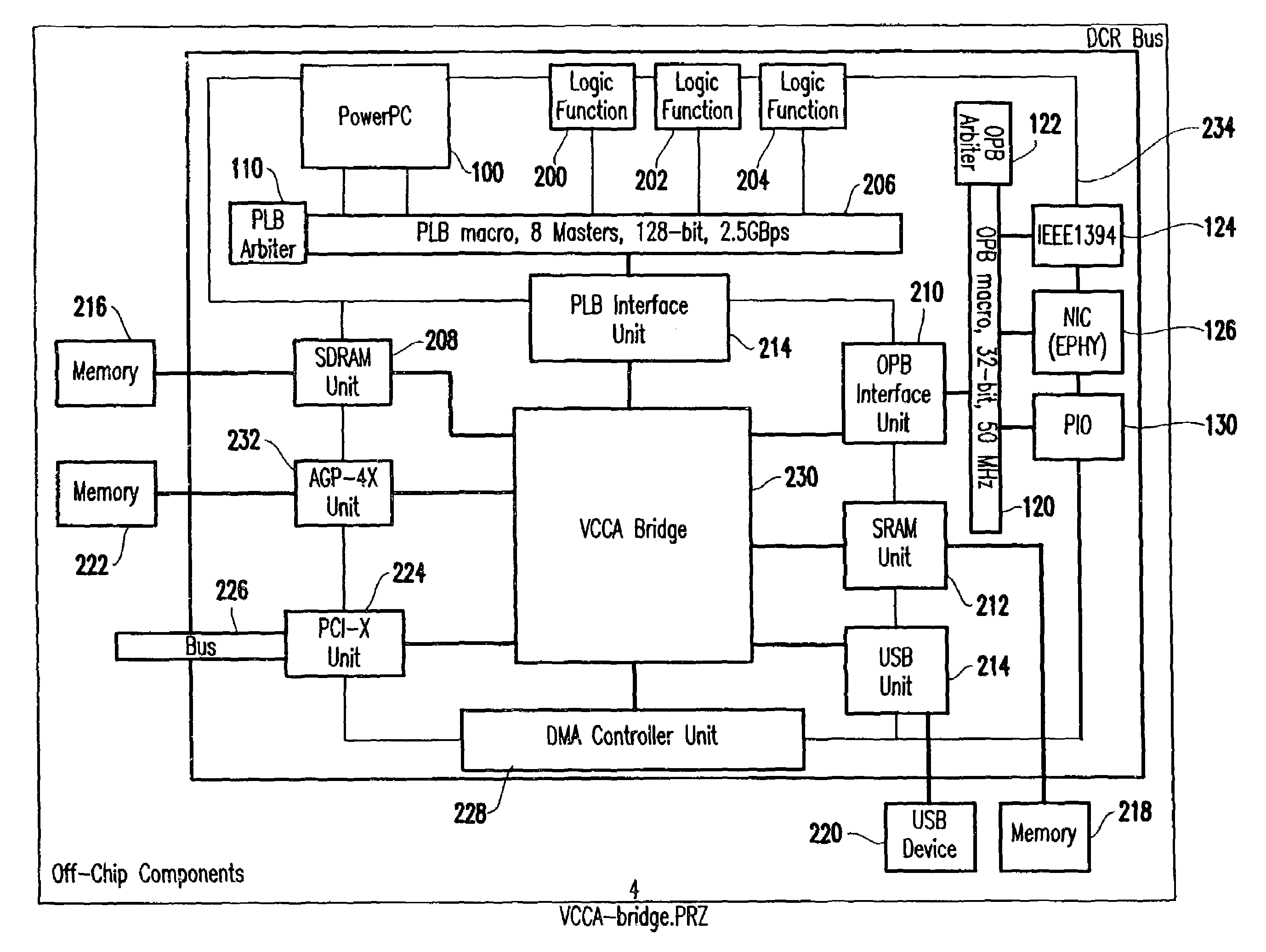
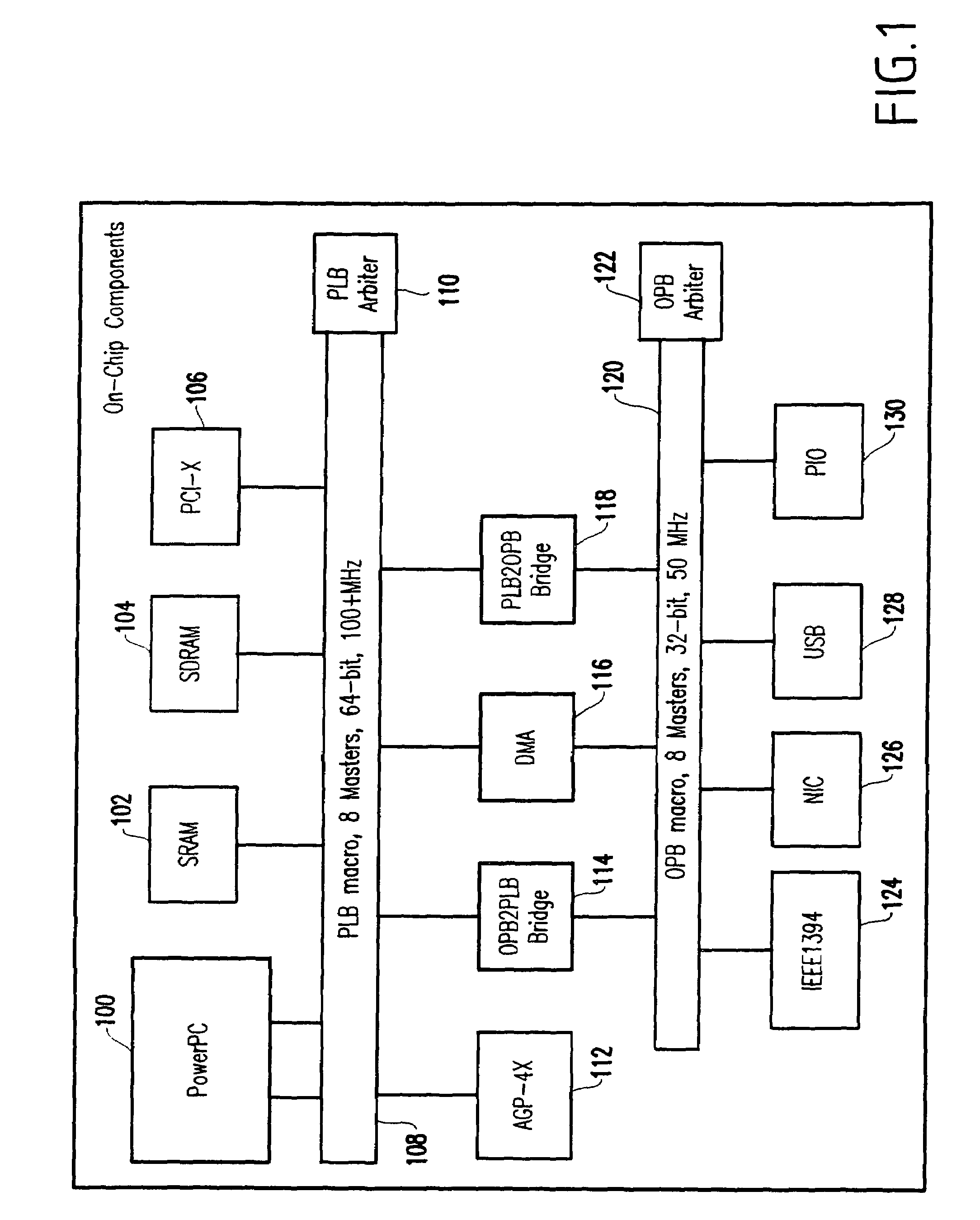
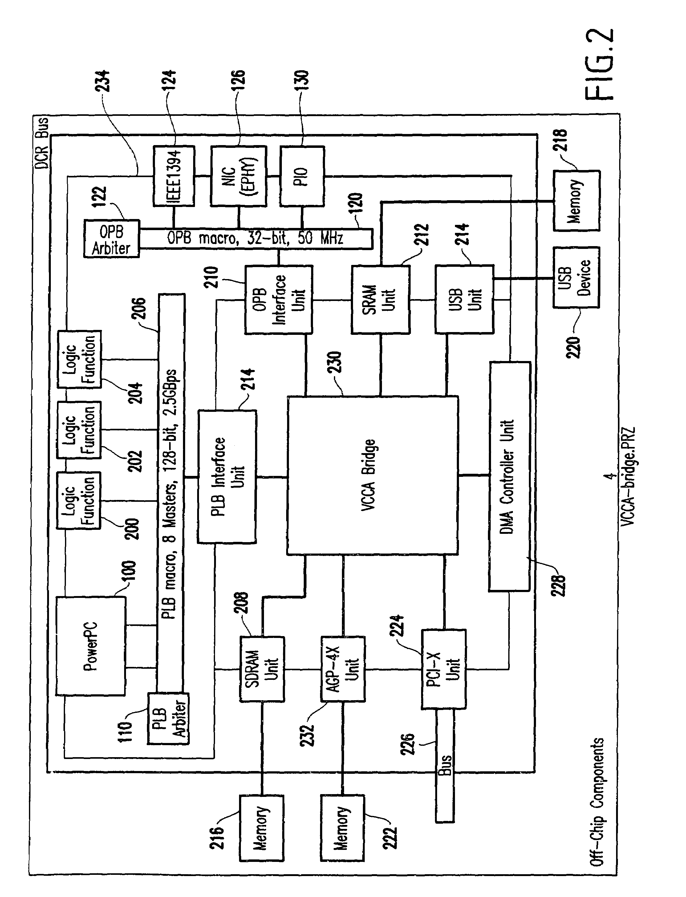
[0014]Referring now to the drawings, and more particularly to FIG. 1, a first System-on-a-Chip (SoC) system is illustrated that includes two buses, a processor local bus (PLB) 108 and an on-chip peripheral bus (OPB) 120. One or more logic devices 100 (such as the PowerPC available from IBM Corporation, Armonk N.Y., USA), are connected to the processor local bus 108. Additionally, memory devices, such as a static random access memory (SRAM) 102 and synchronous dynamic random access memory 104 (SDRAM) are connected to the processor local bus 108. Further, other peripheral interfaces, such as the peripheral component interface (PCI) and an advanced graphic pod (AGP) 112 are connected to the processor local bus 108. Various peripheral devices such as the IEEE1394 serial interface 124, network interface card (NIC) 126, universal serial bus (USB) 120, and a programmable input / output (PIO) are connected to the on-chip peripheral bus 120.

[0015]In operation, the PLB arbiter 110 and the OPB a...


PUM


Abstract

A system-on-a-chip integrated circuit structure includes a bridge having a plurality of channels, a processor local bus connected to the bridge (wherein the bridge includes a first channel dedicated to the processor local bus), at least one logic device connected to the processor local bus, a peripheral device bus connected to the bridge (wherein the bridge includes a second channel dedicated to the peripheral device bus), at least one peripheral device connected to the peripheral device bus, at least one memory unit connected to the bridge (wherein the bridge includes a third channel dedicated to the memory unit), and at least one input/output unit connected to the bridge (wherein the bridge includes a fourth channel dedicated to the input/output unit).

Description

BACKGROUND OF THE INVENTION[0001]1. Field of the Invention[0002]The present invention generally relates to System-on-a-Chip architecture and more particularly to an improved bridge that provides multiple virtual channels for the devices connecting to the bridge to reduce latencies.[0003]2. Description of the Related Art[0004]Conventional component-based System-on-a-Chip (SoC) communication architectures achieve poor performance. This is primarily due to the blocking nature of their on-chip communication structures associated with handshake protocols, interconnecting processors and their peripheral Intellectual Property (IP) blocks, which induces latencies that degrade performances of bus system hierarchies. Existing chipset bridges connect processors running at clock speeds of 500 MHz or more to system memories and to I / O's that operate at much lower speed, typically below 100 MHz. Conventionally, the main memory subsystems (fast DRAM) offer high throughput, but they often require s...

Claims


Application Information

Patent Timeline
IPC IPC(8): G06F13/14
CPCG06F13/4027
Inventor NSAME, PASCAL A.
Owner GLOBALFOUNDRIES US INC
Why Eureka
Try Eureka