Integrated circuit-based compound eye image sensor using a light pipe bundle

a technology of compound eye and light pipe bundle, which is applied in the field of integrated circuit-based compound eye image sensor, can solve the problems of limited scale of these devices, single lens system not scaling well to small size, and limited utility of single lens system

Inactive Publication Date: 2006-01-17
INTEL CORP
View PDF9 Cites 84 Cited by
  • Summary
  • Abstract
  • Description
  • Claims
  • Application Information

AI Technical Summary

Problems solved by technology

In some cases, however, currently available technology limits the extent to which these devices may be scaled.
Such single lens systems do not scale well to small sizes and weights, however, due to issues such as lens curvature and focal length, for example, and thus, their utility may be limited for current and / or future applications where very small and / or lightweight image sensing components are desired.

Method used


Image

  • Integrated circuit-based compound eye image sensor using a light pipe bundle
  • Integrated circuit-based compound eye image sensor using a light pipe bundle
  • Integrated circuit-based compound eye image sensor using a light pipe bundle

Examples


Embodiment Construction

[0020]A method and apparatus for image sensing using an integrated circuit-based compound eye is described. In the following description, particular types of integrated circuits, lens configurations and materials, for example are described for purposes of illustration. It will be appreciated, however, that other embodiments are applicable to other types of integrated circuits, and to light directing elements and / or image sensors configured in another manner.

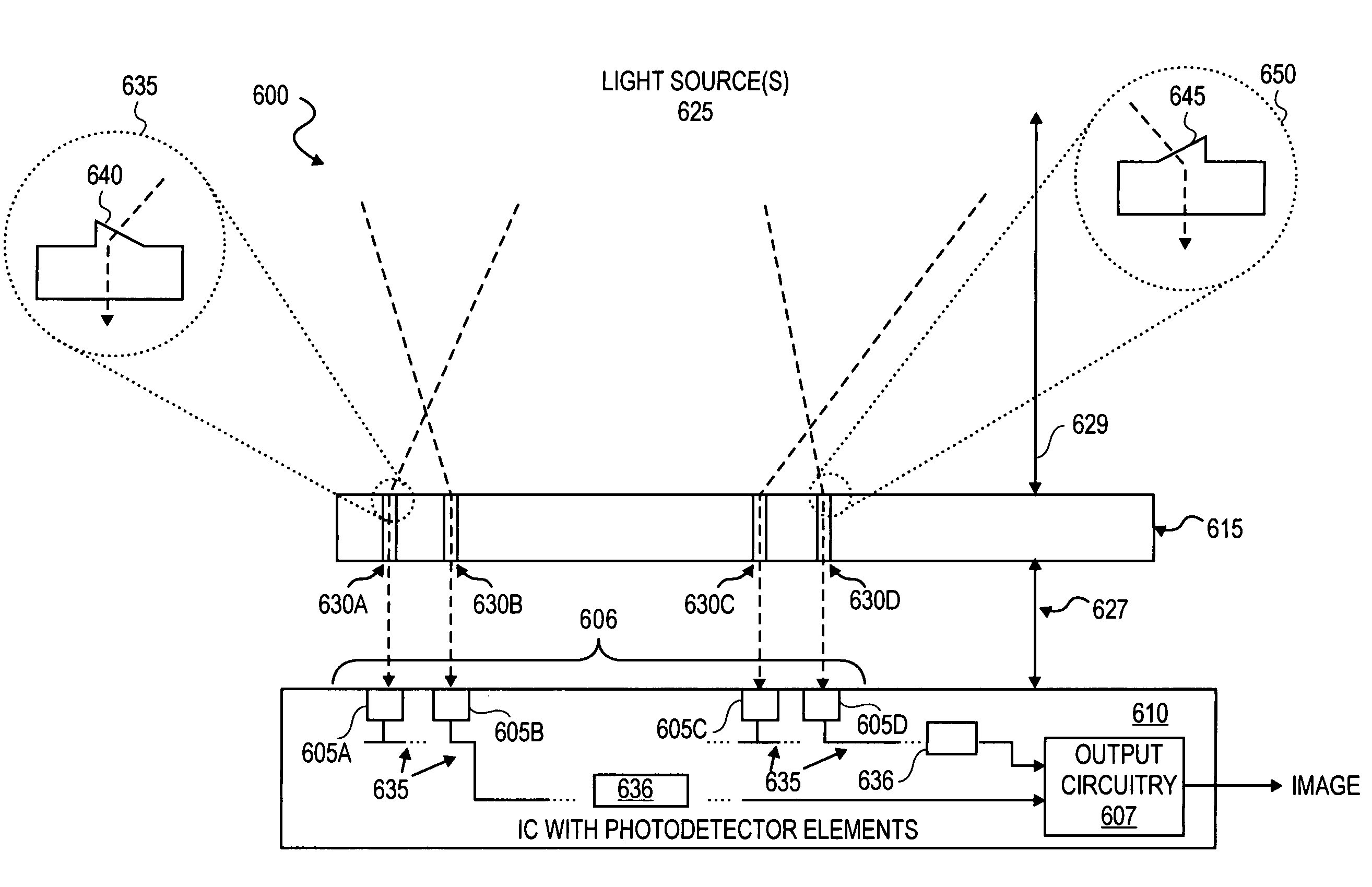
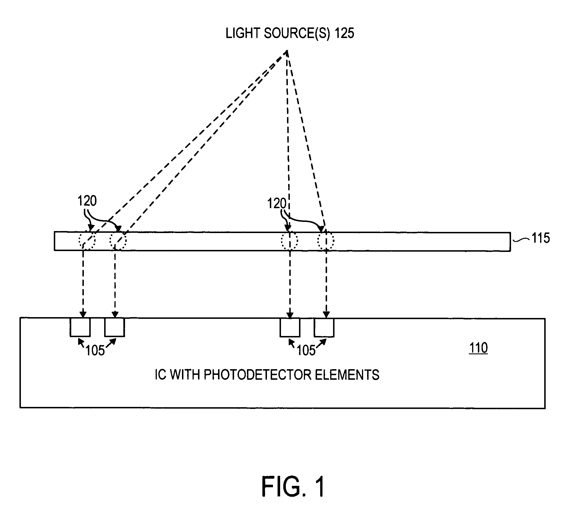
[0021]For one embodiment, referring to FIG. 1, an apparatus comprises a plurality of photodetector elements 105 (also referred to herein as pixels, light receptor, photoreceptor and / or optoelectronic elements) disposed on a substrate 110, such as a semiconductor substrate. The apparatus also includes a light directing member 115, also referred to herein as an exposure determining member, including a plurality of light directing elements 120 (only a few of which are indicated in FIG. 1).

[0022]For this embodiment, at least some of ...


PUM


Abstract

An integrated circuit-based compound eye includes a plurality of photodetector elements disposed on a semiconductor substrate. A compound light directing member includes a light pipe bundle wherein at least some of the light pipes are to individually direct light energy from one or more sources onto one or more of the photodetector elements. The compound light directing member is the primary mechanism to direct light energy onto the one or more of the photodetector elements. Outputs of the photodetector elements are electrically coupled in such a way that an image associated with the source may be synthesized at output circuitry.For another aspect, a compound exposure determining member includes a plurality of light scanning elements, each of the light scanning elements including an integrated photodetector. Each of the light scanning elements is controllable to vary an angle of the photodetector with respect to a substrate to determine from which point sources and angles light energy is received at the photodetector.

Description

BACKGROUND[0001]1. Field[0002]An embodiment of the present invention relates to the field of imaging devices and methods and, more particularly, to an integrated circuit-based, artificial compound eye.[0003]2. Discussion of Related Art[0004]The market for image sensing devices is growing rapidly as new applications for such devices continue to arise. Current applications include camcorders, facsimile machines, digital cameras, toys and personal computer (PC) cameras, for example. Cameras and / or other types of image sensing devices are also expected to soon be included in items such as cars, wireless telephones, and personal digital assistants, for example.[0005]For many applications, there is a drive to continue to make components, including image sensing components, smaller. In some cases, however, currently available technology limits the extent to which these devices may be scaled. Current cameras, such as PC cameras, for example, typically include a single lens to focus light en...

Claims


Application Information

Patent Timeline
Patent Type & Authority Patents(United States)
IPC IPC(8): H01L27/00G02B3/00H01L31/0232H04N5/335
CPCH04N5/335H04N5/23232H01L31/0232G02B3/0031G02B3/0056H01L31/02325H04N23/951H04N25/00
Inventor MATES, JOHN W.
Owner INTEL CORP
Why Eureka
Try Eureka