Substrate structure of liquid crystal display and fabrication method thereof

a technology of liquid crystal display and substrate structure, which is applied in non-linear optics, instruments, optics, etc., can solve the problems of poor light transmittance, affecting and the complexity of the uniform liquid crystal injection. achieve the effect of improving the light transmittance efficiency of the liquid crystal display panel

Inactive Publication Date: 2006-01-24
LG DISPLAY CO LTD
View PDF3 Cites 37 Cited by
  • Summary
  • Abstract
  • Description
  • Claims
  • Application Information

AI Technical Summary

Benefits of technology

[0058]In order to solve the above-mentioned problems and other problems, it is an object of the present invention to provide a substrate structure of a liquid crystal display and a fabrication method thereof that are capable of improving the light transmittance efficiency of a liquid crystal display panel.

Problems solved by technology

However, if the size of the unit liquid crystal display panel increases, uniform liquid crystal injection become more intricate and productivity is lowered due to liquid crystal injection errors.
Thus, in the conventional liquid crystal display panel, light transmittance is not good.
In addition, because the micro lens 90 adhered to each unit pixel of the liquid crystal display panel increases the weight and thickness of the liquid crystal display panel, it is difficult to lower the weight of the liquid crystal display and slim down the liquid crystal display.
Accordingly, the light transmittance of the liquid crystal display is not remarkably improved in comparison with improvement of light usage efficiency.

Method used


Image

  • Substrate structure of liquid crystal display and fabrication method thereof
  • Substrate structure of liquid crystal display and fabrication method thereof
  • Substrate structure of liquid crystal display and fabrication method thereof

Examples


first embodiment

[0086]FIG. 5 is an exemplary view illustrating a substrate structure of a liquid crystal display in accordance with the present invention.

[0087]As depicted in FIG. 5, the substrate structure includes a substrate 110 having a flat first surface 111, a second surface 113, a light transmission region and a light cut-off region; wirings 112 patterned on the light cut-off region of the first surface 111 of the substrate 110; and cylindrical grooves 116 formed on the second surface 113 of the substrate 110 along the length direction of the wiring 112.

[0088]FIGS. 6A to 6F are exemplary views sequentially illustrating fabrication processes of the substrate structure of the liquid crystal display in accordance with the first embodiment of the present invention.

[0089]First, as depicted in FIG. 6A, the wirings 112 are patterned on the first surface 111 of the substrate 110. In this example, the substrate 110 is a TFT array substrate of a liquid crystal display, and the first surface 111 on whi...

second embodiment

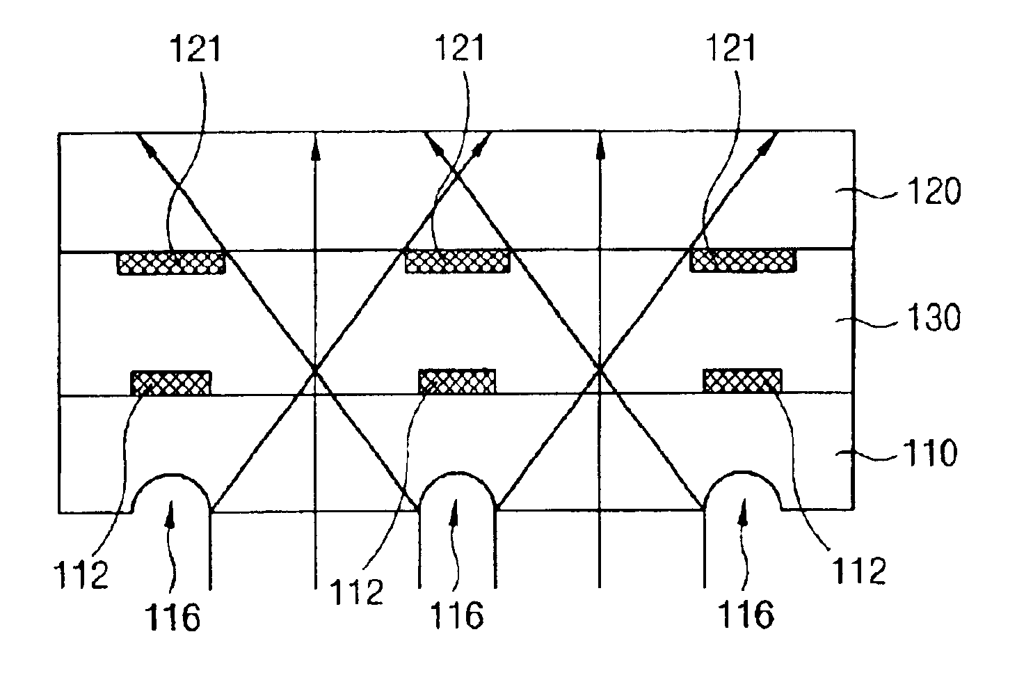
[0107]FIG. 9 is an exemplary view illustrating a substrate structure of a liquid crystal display in accordance with the present invention.

[0108]As depicted in FIG. 9, the substrate structure of the liquid crystal display in accordance with the second embodiment of the present invention includes a first substrate 110 and a second substrate 120 adhered to each other so as to face each other and having a certain space between them; a liquid crystal layer 130 filled into the space between the first substrate 110 and the second substrate 120; wirings 112 and a black matrix 121 respectively patterned on each internal surface of the first substrate 110 and the second substrate 120 so as to face each other; and cylindrical grooves 136 formed at the outer surface of the second substrate 120 on which the black matrix 121 is not formed so as to correspond to the black matrix 121.

[0109]In the substrate structure in FIG. 9, in comparison with the substrate structure of FIG. 7, the light from a l...

third embodiment

[0120]FIG. 11 is an exemplary view illustrating a substrate structure of a liquid crystal display in accordance with the present invention.

[0121]As depicted in FIG. 11, the substrate structure of the liquid crystal display in accordance with the third embodiment of the present invention includes a substrate 110 having a flat first surface 111, a second surface 113, a light transmission region and a light cut-off region; wirings 112 patterned on the light cut-off region of the first surface 111 of the substrate 110; and cylindrical protrusions 156 formed on the second surface 113 of the substrate 110 and extending along the length direction of the wirings 112.

[0122]FIGS. 12A to 12F are exemplary views sequentially illustrating fabrication processes of the substrate structure of FIG. 11 in accordance with the third embodiment of the present invention.

[0123]First, as depicted in FIG. 12A, the wirings 112 are patterned on the first surface 111 of the substrate 110. In this example, the ...


PUM

PropertyMeasurementUnit
anglesaaaaaaaaaa
areaaaaaaaaaaa
light transmittanceaaaaaaaaaa

Abstract

In a substrate structure and a fabrication method thereof, light refracting members aligned with wirings or black matrix formed are integrally formed at a surface of a substrate. Light incident on the wirings or the black matrix can be refracted to a pixel region of the liquid crystal display panel. Accordingly, a flux of light being transmitted through the pixel region of the liquid crystal display panel can be improved significantly.

Description

[0001]The present application claims the benefit of Korean Patent Application No. 88578 / 2001 filed Dec. 29, 2001, under 35 U.S.C. § 119, which is herein fully incorporated by reference.BACKGROUND OF THE INVENTION[0002]1. Field of the Invention[0003]The present invention relates to a substrate structure of a liquid crystal display and a fabrication method thereof, and in particular to a substrate structure of a liquid crystal display and a fabrication method thereof that are capable of improving the light transmittance of the liquid crystal display.[0004]2. Description of the Background Art[0005]In general, liquid crystal display is for displaying pictures by adjusting the light transmittance of liquid crystal cells. Data signals according to picture information are supplied to the liquid crystal cells individually arranged in a matrix form.[0006]The liquid crystal display includes a liquid crystal display panel having pixel unit liquid crystal cells in a matrix form and a driver IC ...

Claims


Application Information

Patent Timeline
Patent Type & Authority Patents(United States)
IPC IPC(8): G02F1/1335G02F1/1333
CPCG02F1/133526G02F1/133512G02F1/1333
Inventor CHAE, GEE-SUNG
Owner LG DISPLAY CO LTD
Why Eureka
Try Eureka