Electrical circuit board and a method for making the same

a technology of electrical circuit board and circuit board, which is applied in the direction of printed circuit, cable/conductor manufacturing, printed element electric connection formation, etc., can solve the problems of defective portion or region of the circuit board, the failure of the solder to electrically connect the desired layers of circuitry and/or components together, and the failure of the solder to consistently and reliably achieve the effect of high reliability and solderability

Inactive Publication Date: 2006-02-14
VISTEON GLOBAL TECH INC
View PDF11 Cites 11 Cited by
  • Summary
  • Abstract
  • Description
  • Claims
  • Application Information

AI Technical Summary

Benefits of technology

[0009]It is a second object of the present invention to provide a method for making a multi-layer electrical circuit board which includes one or more vias, apertures or cavities which provide for highly reliable and solderable interconnections between conductive layers or portions of the circuit board.
[0010]It is a third object of the invention to provide a method for producing a multi-layer electrical circuit board which overcomes some or all of the previously delineated drawbacks of prior multi-layer electrical circuit board forming methodologies and techniques and which allows for the selective, efficient, and reliable formation of apertures or cavities, which allows for communication by and between some or all of the various component containing surfaces and portions of the formed multi-layer electrical circuit board, which selectively allows components contained within and / or upon these portions and surfaces to be interconnected, and which is further adapted to selectively and communicatively receive an electrical component and / or an electrical component connector portion.

Problems solved by technology

One drawback associated with these conventional vias and with this circuit board design is that layers of relatively non-solderable material (i.e., insulating material and / or material which does not substantially bind or metallurgically bond with solder) are typically present within these vias, and thus, the solder does not consistently and reliably electrically connect the desired layers of circuitry and / or components together.
This arrangement often results in a void which is not filled by the relatively high-tension solder material, thereby substantially preventing or reducing the likelihood of the solder material “wetting” or metallurgically bonding to the conducting portions or layers of the circuit board.
Hence, these types of arrangements often result in a defective portion or region of the circuit board where all layers of the circuit board are not desirably interconnected.

Method used


Image

  • Electrical circuit board and a method for making the same
  • Electrical circuit board and a method for making the same
  • Electrical circuit board and a method for making the same

Examples


second embodiment

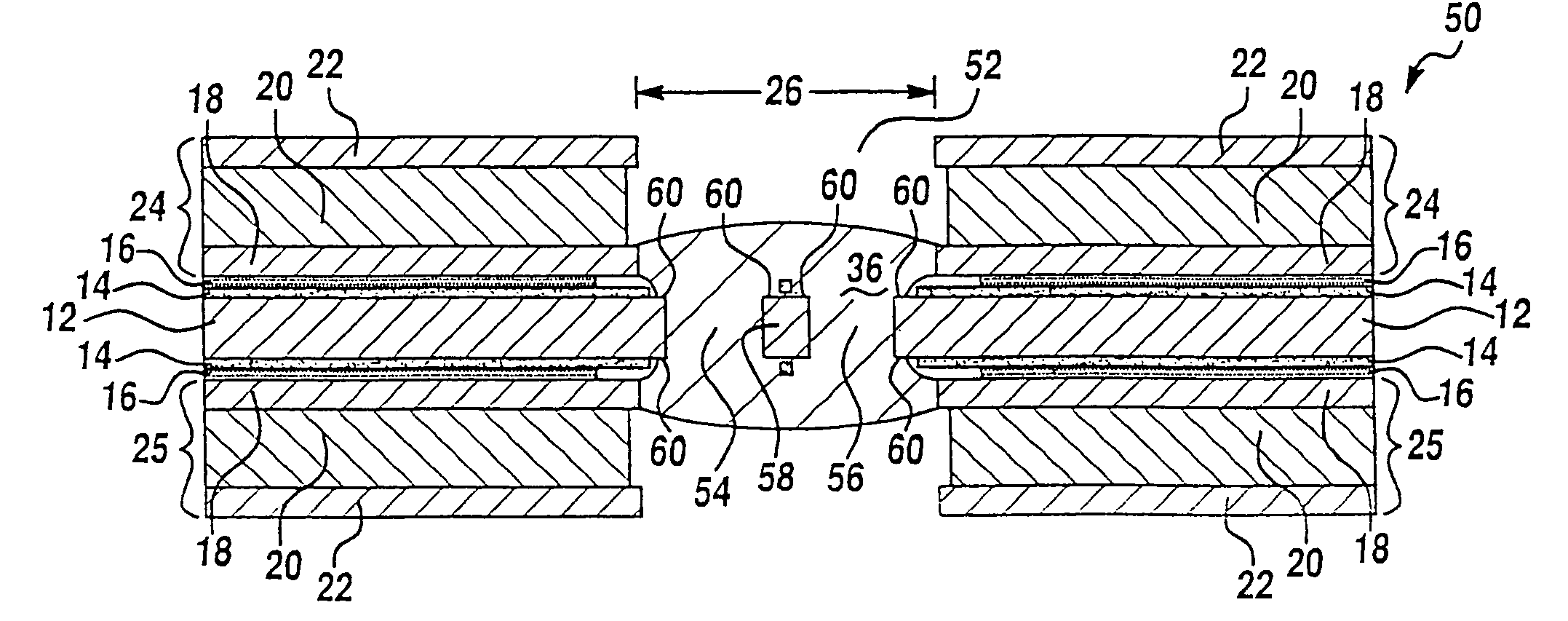
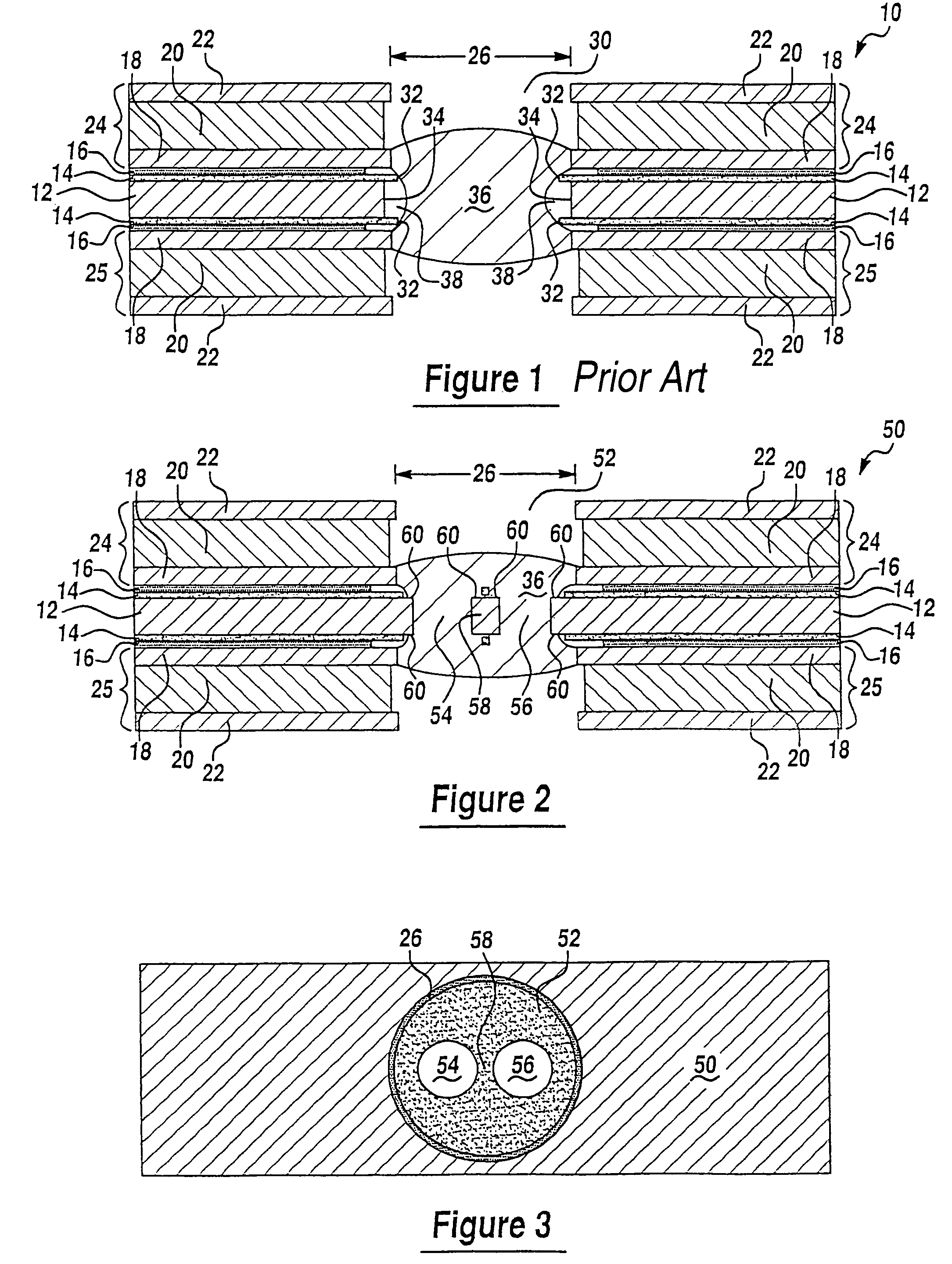
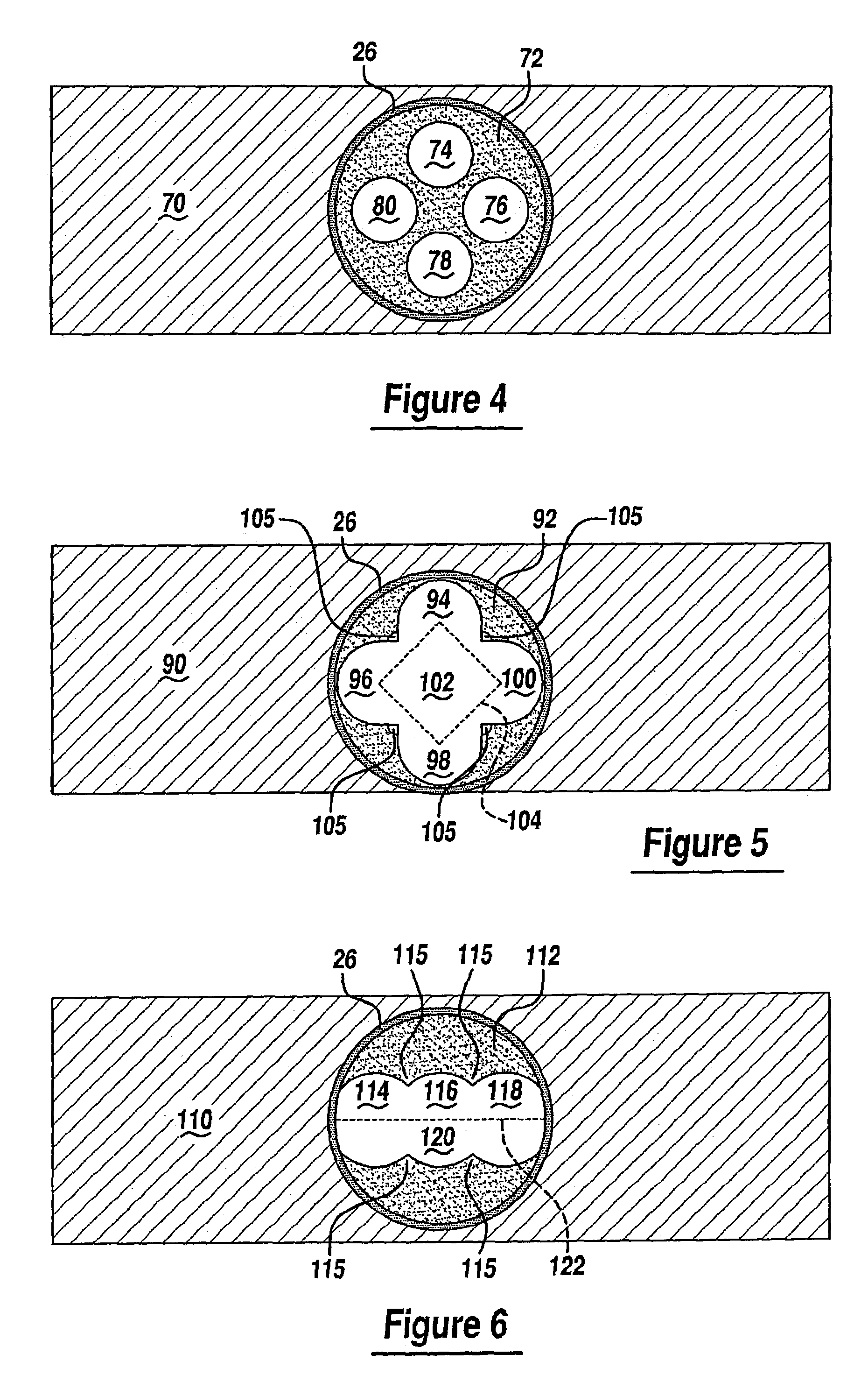
[0032]Referring now to FIG. 4, there is shown a circuit assembly 70 made in accordance with the teachings of the present invention. Circuit assembly 70 is substantially identical to circuit assembly 50 with the exception that via or aperture 52 has been replaced with via or aperture 72.

[0033]Via or aperture 72 includes four holes or apertures 74, 76, 78 and 80 which are formed within dielectric layers 14 and core 12. Apertures 74, 76, 78 and 80 are formed by a conventional machining process such as drilling, laser ablation, routing, stamping, cutting or punching and are formed in relative close proximity to each other. In alternate embodiments, apertures 74–80 may be formed by an etching or chemical milling process. When apertures 74–80 are machined, the relatively brittle dielectric coating 14 chips, flakes or otherwise separates off of the end portions or corner regions of core 12, in a manner substantially similar to that described in reference to circuit assembly 50. The formati...

third embodiment

[0034]Referring now to FIG. 5, there is shown a circuit assembly 90 made in accordance with the teachings of the present invention. Circuit assembly 90 is substantially identical to circuit assembly 70 with the exception that via or aperture 72 has been replaced with via or aperture 92.

[0035]Via or aperture 92 includes four intersecting and generally circular holes 94, 96, 98, and 100 which interconnect and / or overlap to form one hole or aperture 102 within dielectric layers 14 and core 12. Apertures 94, 96, 98, and 100 are formed by a conventional machining process, such as drilling, routing, stamping, cutting, punching, or laser ablation and are formed in a substantially “square” arrangement as indicated by dashed line 104 (e.g., the center of each aperture 13 located at the four corners of square 104). In alternate embodiments, apertures 74–80 may be found by an etching or chemical milling process. When apertures 94–100 are machined, the relatively brittle dielectric coating 14 c...

fourth embodiment

[0036]Referring now to FIG. 6, there is shown a circuit assembly 110 made in accordance with the teachings of the present invention. Circuit assembly 110 is substantially identical to circuit assembly 90 with the exception that via or aperture 92 has been replaced with via or aperture 112.

[0037]Via or aperture 112 includes three intersecting and generally circular holes 114, 116, and 118 which interconnect and / or overlap to form one hole or aperture 120 within dielectric layers 14 and core 12. Apertures 114, 116, and 118 are formed by a conventional etching or machining process, such as drilling, routing, stamping, cutting, punching or laser ablation and are formed in a substantially linear arrangement as indicated by dashed line 122. When apertures 114–118 are machined, the relatively brittle dielectric coating 14 chips, flakes or otherwise separates off of the end portions or corner regions of core 12, in a manner substantially similar to that described with reference to circuit a...


PUM

PropertyMeasurementUnit
conductiveaaaaaaaaaa
perimeteraaaaaaaaaa
electrical poweraaaaaaaaaa

Abstract

A multi-layer electronic circuit board design 10 having selectively formed apertures or cavities 26 which have improved solder-wetting characteristics.

Description

[0001]“This application is a division of application Ser. No. 09 / 655,985 filed on Sep. 6, 2000, U.S. Pat. No. 6,585,903”.FIELD OF THE INVENTION[0002]The present invention relates to a method for making an electrical circuit board and more particularly, to a method for making a multi-layer electrical circuit board having apertures and / or cavities which are formed within the circuit board and / or through various portions of the circuit board, and which provide for improved and / or more reliable solder interconnections between portions or layers of the circuit board.BACKGROUND OF THE INVENTION[0003]Multi-layer circuit boards contain and / or include electrical components and interconnecting conductive traces or routing lines which selectively and operatively populate opposed first and second surfaces (i.e., top and bottom surfaces) of each board (or other respective interior portions of each of the boards), thereby desirably allowing each of the electrical circuit boards to contain and / or ...

Claims


Application Information

Patent Timeline
Patent Type & Authority Patents(United States)
IPC IPC(8): H01R12/04H05K3/40H05K3/44
CPCH05K3/4038H05K3/44H05K2201/0305H05K2201/0361H05K2201/09554Y10T29/49126H05K2201/0979H05K2201/09854Y10T29/49124Y10T29/49156H05K2201/09745
Inventor BELKE, JR., ROBERT EDWARDJAIRAZBHOY, VIVEK A.KRAUTHEIM, THOMAS B.QUITTY, JR., WILLIAM F.
Owner VISTEON GLOBAL TECH INC
Why Eureka
Try Eureka