Semiconductor memory device

a memory device and semiconductor technology, applied in the field of semiconductor memory devices, can solve the problems of difficult decoder layout, weak probability of wiring penalties, and inapplicability of techniques, so as to reduce the probability of wiring penalties and facilitate the arrangement of decoders

Inactive Publication Date: 2006-02-14
SOCIONEXT INC
View PDF22 Cites 0 Cited by
  • Summary
  • Abstract
  • Description
  • Claims
  • Application Information

AI Technical Summary

Benefits of technology

[0029]In order to address such problems, the present invention was made. An object of the present invention is to reduce the probability of the penalties of wirings arising and to make the arrangement of decoders easy, especially in a semiconductor memory device having a plurality of subblocks.

Problems solved by technology

Therefore, as shown in FIGS. 13 and 14, some of these wirings must pass over a subblock, resulting in a stronger probability of the penalties of wirings arising and difficulty in a decoder layout.
However, this technique is not applicable to cases where more than two memory arrays exist.

Method used


Image

  • Semiconductor memory device
  • Semiconductor memory device
  • Semiconductor memory device

Examples


second embodiment

[0085]the present invention will now be described.

[0086]FIG. 5 is a view for giving an overview of a second embodiment of the present invention. As shown in FIG. 5, a semiconductor memory device according to the second embodiment comprises memory arrays 60a and 61a, decoding circuits 60b and 61b, fuse circuits 60c and 61c, and wirings 60d and 61d.

[0087]The first through fifth columns from the left of the memory array 60a, decoding circuit 60b, fuse circuit 60c, and wiring 60d form a subblock and the sixth through tenth columns from the left of them form another one.

[0088]Moreover, the first through fifth columns from the left of the memory array 61a, decoding circuit 61b, fuse circuit 61c, and wiring 61d form a subblock and the sixth through tenth columns from the left of them form another one.

[0089]In this example, only four subblocks are shown to simplify descriptions, but in practice more than four subblocks can exist.

[0090]The memory arrays 60a and 61a include a plurality of me...

third embodiment

[0102]the present invention will now be described.

[0103]FIG. 7 is a view showing the structure of a third embodiment of the present invention. The third embodiment is a synthesis of the first and second embodiments. In this example, a semiconductor memory device according to the third embodiment comprises a subblock 65 and subblock 66. As shown in FIG. 5, two or more subblocks may exist in the horizontal direction.

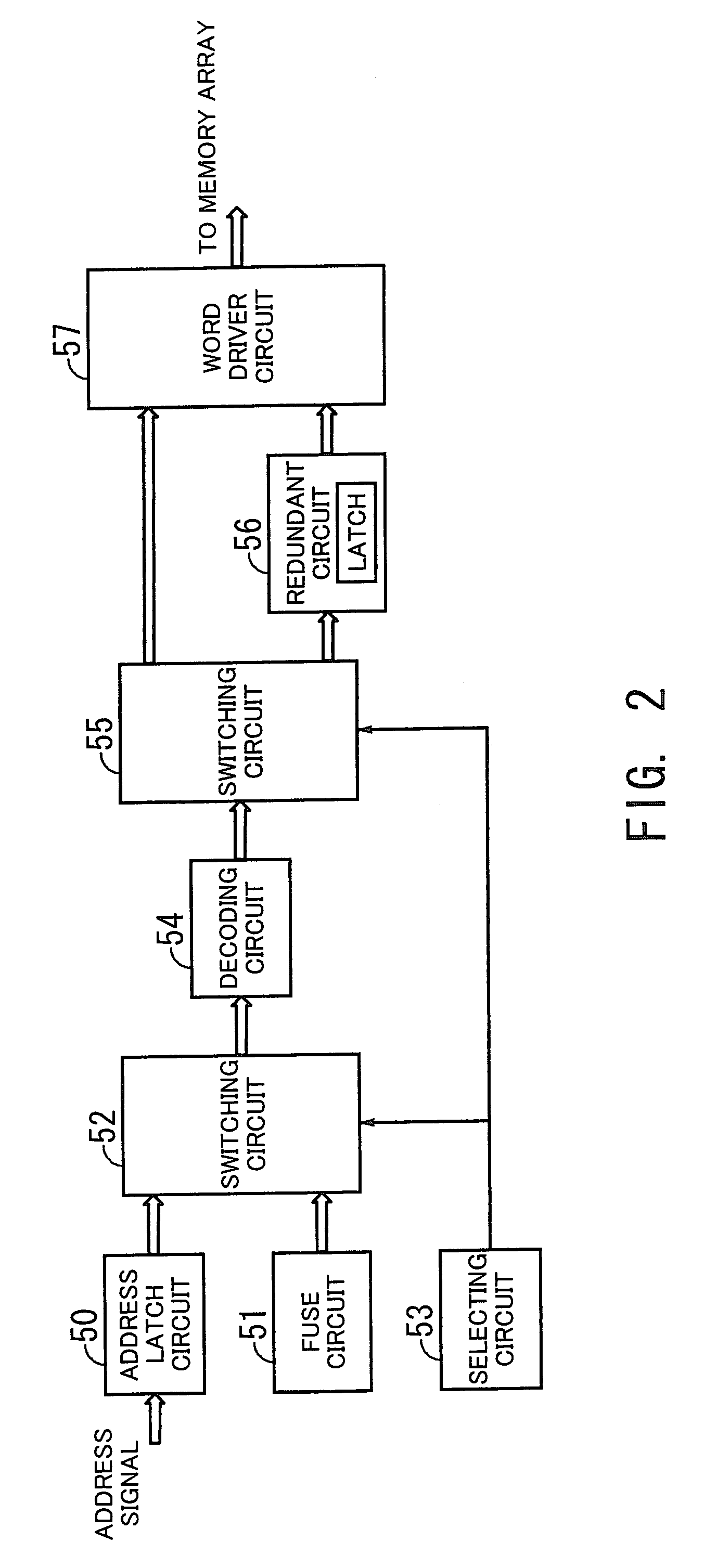
[0104]FIG. 8 is an enlarged view of an area enclosed with a dashed line in FIG. 7. In this example, the area includes an address latch circuit 70, a fuse circuit 71, a selecting circuit 72, a switching circuit 73, decoding circuits 74a and 75a, switching circuits 74b and 75b, latch circuits 74c and 75c, redundant circuits 74d and 75d, word driver circuits 74e and 75e, and memory cells 74f and 75f.

[0105]The address latch circuit 70, fuse circuit 71, selecting circuit 72, switching circuit 73, decoding circuits 74a and 75a, switching circuits 74b and 75b, redundant circuits...


PUM


Abstract

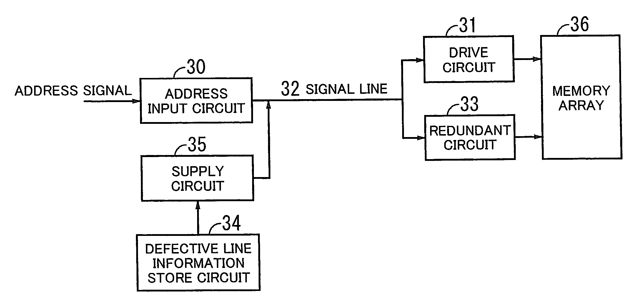
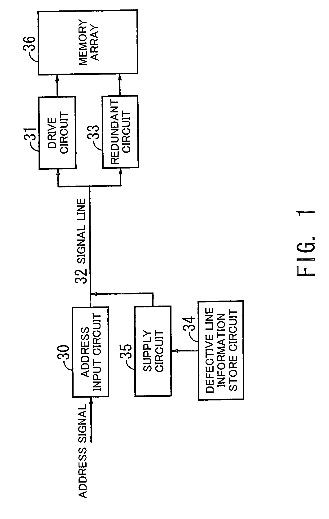
A semiconductor memory device that reduces the probability of the penalties of wirings arising. An address input circuit receives an address signal input. A drive circuit drives a memory array in compliance with the address signal. A signal line connects the address input circuit and the drive circuit. A redundant circuit is located near the drive circuit and substitutes other lines including a redundant line for a defective line in the memory array. A defective line information store circuit stores information showing the defective line. A supply circuit supplies information stored in the defective line information store circuit to the redundant circuit via the signal line. This structure enables to transmit an address signal and information regarding a defective line by a common signal line and to reduce the number of wirings and the probability of the penalties of wirings arising.

Description

[0001]This is a Divisional of application Ser. No. 09 / 988,614 filed Nov. 20, 2001 now U.S. Pat. No. 6,654,298. The disclosure of the prior application(s) is hereby incorporated by reference herein in its entirety.BACKGROUND OF THE INVENTION[0002](1) Field of the Invention[0003]This invention relates to a semiconductor memory device and, more particularly, to a semiconductor memory device having a shift redundancy function.[0004](2) Description of the Related Art[0005]If there is a defective line in a semiconductor memory device manufactured, it can be returned to normal by substituting other lines including a redundant line for the defective line by the use of a technique called shift redundancy.[0006]FIG. 9 is a view for giving an overview of shift redundancy. In FIG. 9, a memory array 2 includes an ordinary line 2a and redundant line 2b. How to connect them is managed by a decoder 1.[0007]As shown in FIG. 10, it is assumed that a defective line is detected in the middle area of th...

Claims


Application Information

Patent Timeline
Patent Type & Authority Patents(United States)
IPC IPC(8): G11C7/00G11C5/06G11C7/02G11C8/00G11C29/04G11C29/00
CPCG11C29/80G11C29/848G11C29/00
Inventor YAGISHITA, YOSHIMASAUCHIDA, TOSHIYA
Owner SOCIONEXT INC
Why Eureka
Try Eureka