

Integrated circuit package employing a flexible substrate
a flexible substrate and integrated circuit technology, applied in the direction of electrical equipment, semiconductor devices, semiconductor/solid-state device details, etc., can solve the problems of increased package thickness, increased risk of overheating, increased footprint of the package, etc., to reduce the footprint of the integrated circuit, reduce the penalty, and facilitate the effect of conducting
- Summary
- Abstract
- Description
- Claims
- Application Information
AI Technical Summary
Benefits of technology
Problems solved by technology
Method used
Image

Examples
Embodiment Construction
[0021] The making and using of the presently preferred embodiments are discussed in detail below. It should be appreciated, however, that the present invention provides many applicable inventive concepts that can be embodied in a wide variety of specific contexts. The specific embodiments discussed are merely illustrative of specific ways to make and use the invention, and do not limit the scope of the invention.
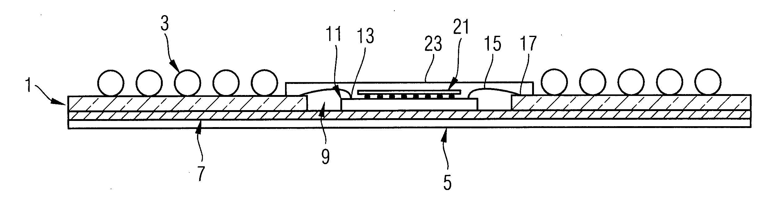
[0022] Referring first to FIG. 1, the embodiment of the invention is shown as being a package composed of a substrate 1, which is laminar and composed of a flexible material. The substrate material is preferably polyimide, but alternatively can be any other material such as olyester, fluorocarbon films, aramid papers, and composites. The upper surface of the substrate 1 (as shown in FIG. 1) is provided with eutectic solder balls 3.
[0023] On one face of the substrate 1 (the lower face, as shown in FIG. 1; i.e., the side opposite the solder balls 3), is mounted a layer 5 of ...
PUM
 Abstract
Description
Claims
Application Information