Flat panel display

a flat panel display and active matrix technology, applied in the field of active matrix flat panel display, can solve the problems of reducing the life cycle of the el device, reducing the size of the anode electrode in the amoled of 180 ppi, and unable to fabricate high-resolution panels, so as to achieve the effect of extending the life cycle and obtaining proper luminan

Inactive Publication Date: 2006-02-21
SAMSUNG DISPLAY CO LTD
View PDF5 Cites 5 Cited by
  • Summary
  • Abstract
  • Description
  • Claims
  • Application Information

AI Technical Summary

Benefits of technology

[0014]Therefore, in order to solve the foregoing problems of the prior art, it is an object of the present invention to provide an active matrix organic light emitting diode capable of obtaining proper luminance and extending life cycle.
[0015]It is another object of the present invention to provide an active matrix organic light emitting diode capable of obtaining a proper luminance per unit area by controlling the amount of current flowing to an organic electroluminescent device.
[0016]It is another object of the present invention to provide an active matrix organic light emitting diode capable of obtaining luminance suitable for display devices by changing resistance value of driving transistor, thereby controlling the amount of current flowing to an organic electroluminescent device.
[0017]It is still another object of the present invention to provide a high-speed flat panel display capable of obtaining a proper luminance by switching operating switching transistor at high-speed and controlling current flowing to the organic electroluminescent device by driving transistor.

Problems solved by technology

Although an active matrix organic light emitting diode (AMOLED) that is a flat panel display gradually requires a high-resolution panel, there have been much difficulties fabricating the high-resolution panel due to characteristics of the organic electroluminescent device and the driving transistor for driving the organic electroluminescent device.
The amount of current flowing to the EL device through the driving transistor is increased, and luminance is excessively increased since size of pixel is reduced to result in a reduction of size of the anode electrode in an AMOLED of 180 ppi or more.
Finally, there are problems in the AMOLED of 180 ppi or more that life cycle of the EL device is reduced as current density per unit area is increased.
Therefore, there are problems in that on current of the driving transistor should be reduced to obtain luminance suitable for an AMOLED of 180 ppi or more.
On the other hand, there are problems of high leakage current although the amount of current flowing to the EL device through the driving transistor can be reduced if a thin film transistor (a-Si TFT) formed of amorphous silicon is applied to driving transistor of the AMOLED.

Method used


Image

  • Flat panel display
  • Flat panel display
  • Flat panel display

Examples


Embodiment Construction

[0044]The present invention will now be described in detail in connection with preferred embodiments with reference to the accompanying drawings. For reference, like reference characters designate corresponding parts throughout several views.

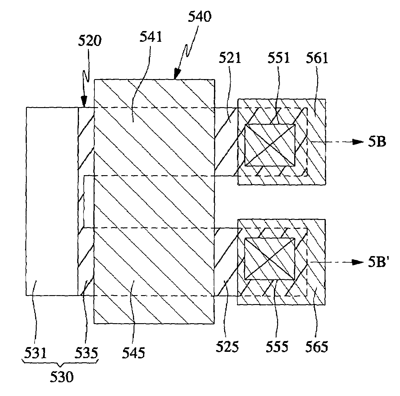
[0045]FIG. 3A to FIG. 3B illustrate plane structure and cross sectional structure of a driving transistor in an organic light emitting diode according to first preferred embodiment of the present invention, wherein the FIG. 3B is a cross sectional view taken along a line 3B–3B′ of FIG. 3A. The driving transistor comprises gate electrode formed as multiple gates and offset region that is high resistance region formed on semiconductor layer between the multiple gates to control the amount of current flowing to an EL device.

[0046]Referring to FIG. 3A and FIG. 3B, the driving transistor according to the first preferred embodiment of the present invention includes semiconductor layer 320, gate electrode 340, and source / drain electrodes 361 and 365. T...


PUM


Abstract

The present invention discloses an organic light emitting diode capable of obtaining proper luminance and long life cycle by controlling an amount of current flowing through an organic electroluminescent device per unit pixel. The organic light emitting diode includes a luminescent device and first and second transistors for driving the luminescent device, wherein the first and second transistors have different resistance values. The first transistor is a driving transistor for driving the luminescent device. The second transistor is a switching transistor for switching on and off the driving transistor. The driving transistor may have a higher resistance value than the switching transistor.

Description

CROSS-REFERENCE TO RELATED APPLICATION[0001]This application claims the benefit of Korean Patent Application No. 2002-61082 filed on Oct. 7, 2003 and Korean Patent Application No. 2003-24508 filed on Apr. 17, 2003, the disclosures of which are hereby incorporated herein by reference in their entirety.BACKGROUND OF THE INVENTION[0002]1. Field of the Invention[0003]The present invention relates to an active matrix flat panel display, more particularly, to an organic light emitting diode capable of generating proper luminance and extending life cycle by controlling the amount of current flowing through an organic electroluminescent (EL) device per unit pixels.[0004]2. Description of Related Art[0005]Although an active matrix organic light emitting diode (AMOLED) that is a flat panel display gradually requires a high-resolution panel, there have been much difficulties fabricating the high-resolution panel due to characteristics of the organic electroluminescent device and the driving tr...

Claims


Application Information

Patent Timeline
Patent Type & Authority Patents(United States)
IPC IPC(8): G09G5/00H05B33/12G09F9/30G09G3/10G09G3/30H01L21/8234H01L27/08H01L27/088H01L27/12H01L27/32H01L29/786H01L51/50H05B33/14
CPCH01L27/1214H01L27/1251H01L29/78618H01L29/78645H01L29/78696H01L27/1222H10K59/12
Inventor PARK, SANG-ILKOO, JAE BON
Owner SAMSUNG DISPLAY CO LTD
Why Eureka
Try Eureka