Two-dimensional redundancy calculation

a two-dimensional redundancy and calculation technology, applied in the field of semiconductor memory devices, can solve the problems of reducing test quality, requiring much more test time, and low yield of insufficient redundancy, and achieve the effect of simplifying the required interaction and less chip area

Active Publication Date: 2006-02-21
TWITTER INC
View PDF20 Cites 20 Cited by
  • Summary
  • Abstract
  • Description
  • Claims
  • Application Information

AI Technical Summary

Benefits of technology

[0010]It is an object of the present invention to provide a large semiconductor memory with BIST implementing two-dimensional redundancy that takes up less chip area and simplifies the required interaction with BIST.

Problems solved by technology

Memories are very dense circuits and are sensitive to subtle defects to which logic circuits are immune.
Further, it is not unusual to see very low yields with insufficient redundancy, sometimes below 1%.
When BIST is employed, as is required in microprocessors and ASICS, the redundancy calculation must be determined on the fly since there is insufficient space to store all the failing locations prior to selecting the redundancy implementation.
Obviously, the amount of circuit overhead to implement these many counters 75 (e.g., approximately 4700 cells for the needed counters and associated clock splitters, etc.), along with the logistical problem of unloading the counters before continuing the BIST testing, create challenges.
This requires much more test time since the information must be sent off chip for each fail.
It also decreases the test quality by having to stop test for each fail rather than providing back-to-back at-speed tests.

Method used


Image

  • Two-dimensional redundancy calculation
  • Two-dimensional redundancy calculation
  • Two-dimensional redundancy calculation

Examples


Embodiment Construction

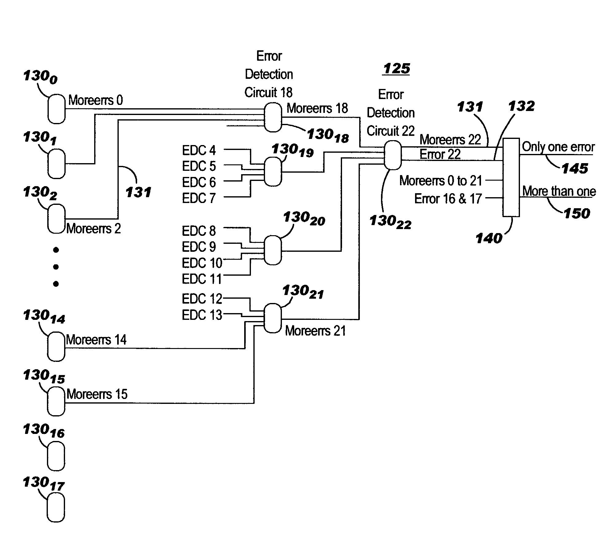
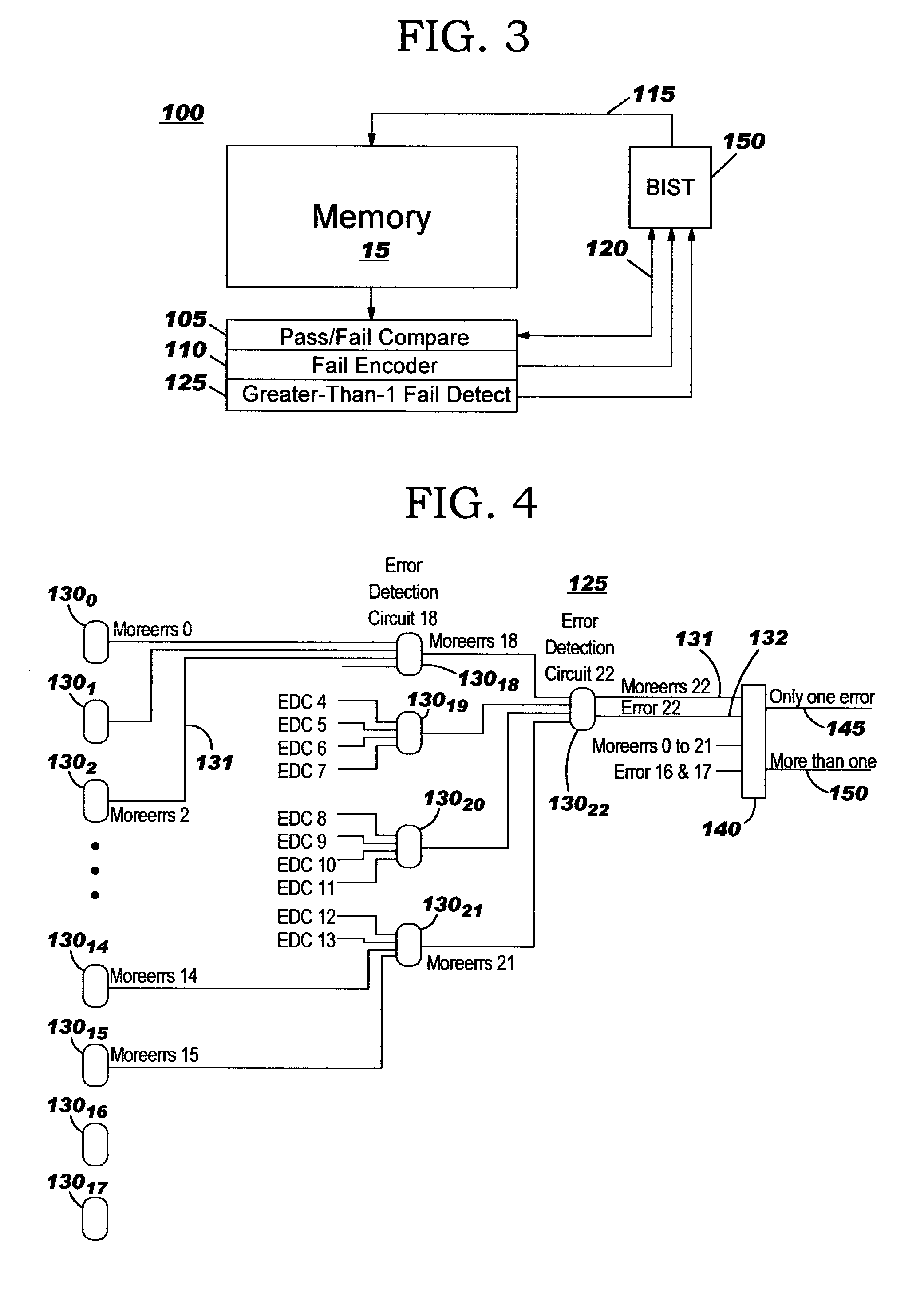
[0023]The present invention is a two-dimensional memory redundancy calculation scheme that provides for a radical reduction in the amount of circuitry required to perform the column redundancy calculation, simplifies the calculation process, and reduces test time.

[0024]FIG. 3 illustrates a high level view of the two-dimensional redundancy calculation system 100 according to the present invention. As shown in FIG. 3, the system components include a normal pass / fail compare circuit 105 which may comprise, for example, the row pass / fail circuitry 20 of FIG. 1, a fail encoder device 110, and a greater-than-one fail detect circuit 125. Each of these components interact with memory 115 and, as shown in FIG. 3, may be separate from the BIST circuitry 150, or, as will be described in greater detail herein, may be integrated within the BIST 150. Particularly, the BIST 150 provides data, address, and control inputs 115 to the memory 15. The BIST additionally includes connection 120 with the p...


PUM


Abstract

A system and methodology for testing memory in an integrated circuit implementing BIST testing to calculate row and column redundancy and enable replacement of a defective row or column of memory cells. The system comprises circuitry for detecting a first single memory cell failure in a row; and, recording the I / O value of the first Single Cell Fail (SCF). A circuit is provided for detecting whether more than one single cell failure has occurred for a tested row, and, in response to detecting a second SCF, comparing recorded I / O value of the subsequent tested row, with the I / O value associated with the first failed memory cell. Upon detection of defective bits, the defective column and row of memory having corresponding defective bits set is replaced.

Description

BACKGROUND OF THE INVENTION[0001]1. Field of the Invention[0002]The present invention relates to semiconductor memory devices employing Built-In-Self-Test (BIST), and particularly, to a novel BIST system and method for calculating redundancy for a two-dimensional redundancy scheme.[0003]2. Description of the Prior Art[0004]Redundancy is required on all large semiconductor memories to ensure adequate chip yield. Memories are very dense circuits and are sensitive to subtle defects to which logic circuits are immune. Thus yield is improved by including redundant elements to replace defective memory portions. As an example, it is not unusual for a chip yield to be 25% without redundancy, 50% with row redundancy, and 70% with two-dimensional (row and column) redundancy. Further, it is not unusual to see very low yields with insufficient redundancy, sometimes below 1%.[0005]Most memories today are embedded so that the memory inputs and outputs (I / O) do not come to the chip I / O. For these ...

Claims


Application Information

Patent Timeline
Patent Type & Authority Patents(United States)
IPC IPC(8): G11C29/00G11C29/40G11C29/44
CPCG11C29/40G11C29/72G11C29/4401G11C29/44
Inventor ADAMS, R. DEANECKENRODE, THOMAS J.GREGOR, STEVEN L.KOCH, GARRETT S.
Owner TWITTER INC
Why Eureka
Try Eureka