Method of making information storage devices by molecular photolithography

a technology of information storage and photolithography, which is applied in the direction of photomechanical equipment, instruments, nuclear engineering, etc., can solve the problems of affecting the quality of the material used, the method of attaching molecules to the surface requires very high concentration, and/or the use of reactive intermediates, etc., and achieves the effect of reducing the number of lithography-based materials, less satisfactory, and avoiding lithography

Inactive Publication Date: 2006-02-28
NORTH CAROLINA STATE UNIV
View PDF8 Cites 37 Cited by
  • Summary
  • Abstract
  • Description
  • Claims
  • Application Information

AI Technical Summary

Problems solved by technology

General challenges in fabricating a hybrid chip containing molecular materials for information storage are that (1) the charge-storage molecule must be attached to an electroactive surface, (2) the electrolyte must be present in the same location as the charge-storage molecule but not elsewhere, (3) the counterelectrode must be located at a controlled distance from the charge-storage molecules.
Particularly pressing problems are that often the methods for attachment of molecules to surfaces require very high concentrations, high temperature, and / or the use of reactive intermediates [Cleland, G. et al., J. Chem. Soc. Faraday Trans.
Such conditions are readily applicable to small robust molecules but become less satisfactory and often fail altogether as the molecules become larger and / or more elaborate.
This procedure also requires very high concentrations for reaction.

Method used


Image

  • Method of making information storage devices by molecular photolithography
  • Method of making information storage devices by molecular photolithography
  • Method of making information storage devices by molecular photolithography

Examples


Embodiment Construction

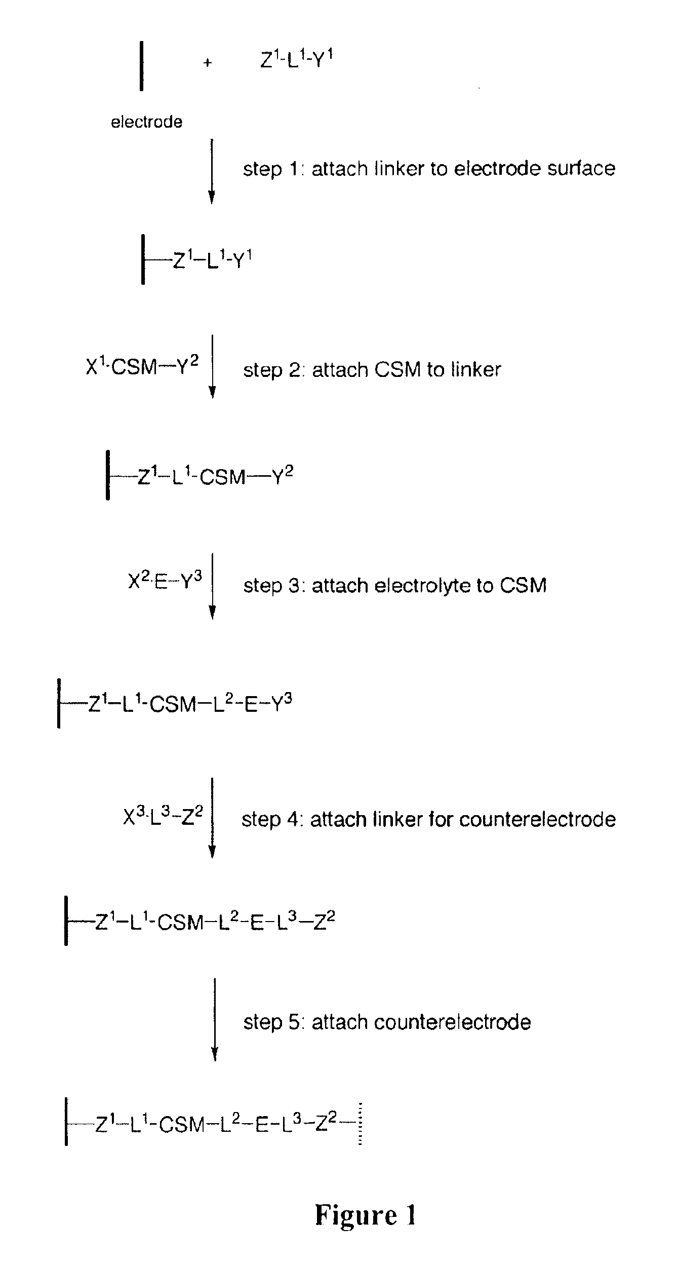
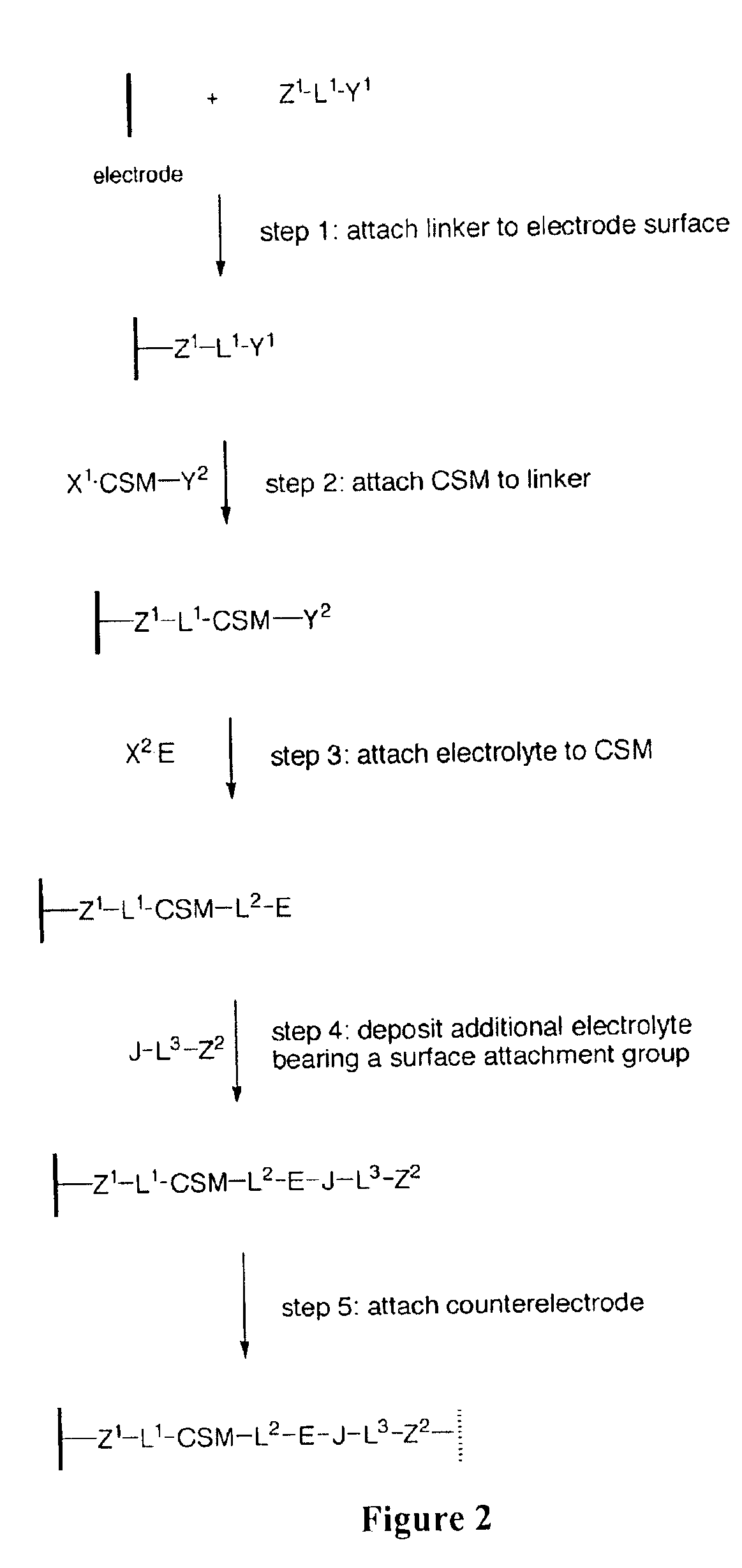
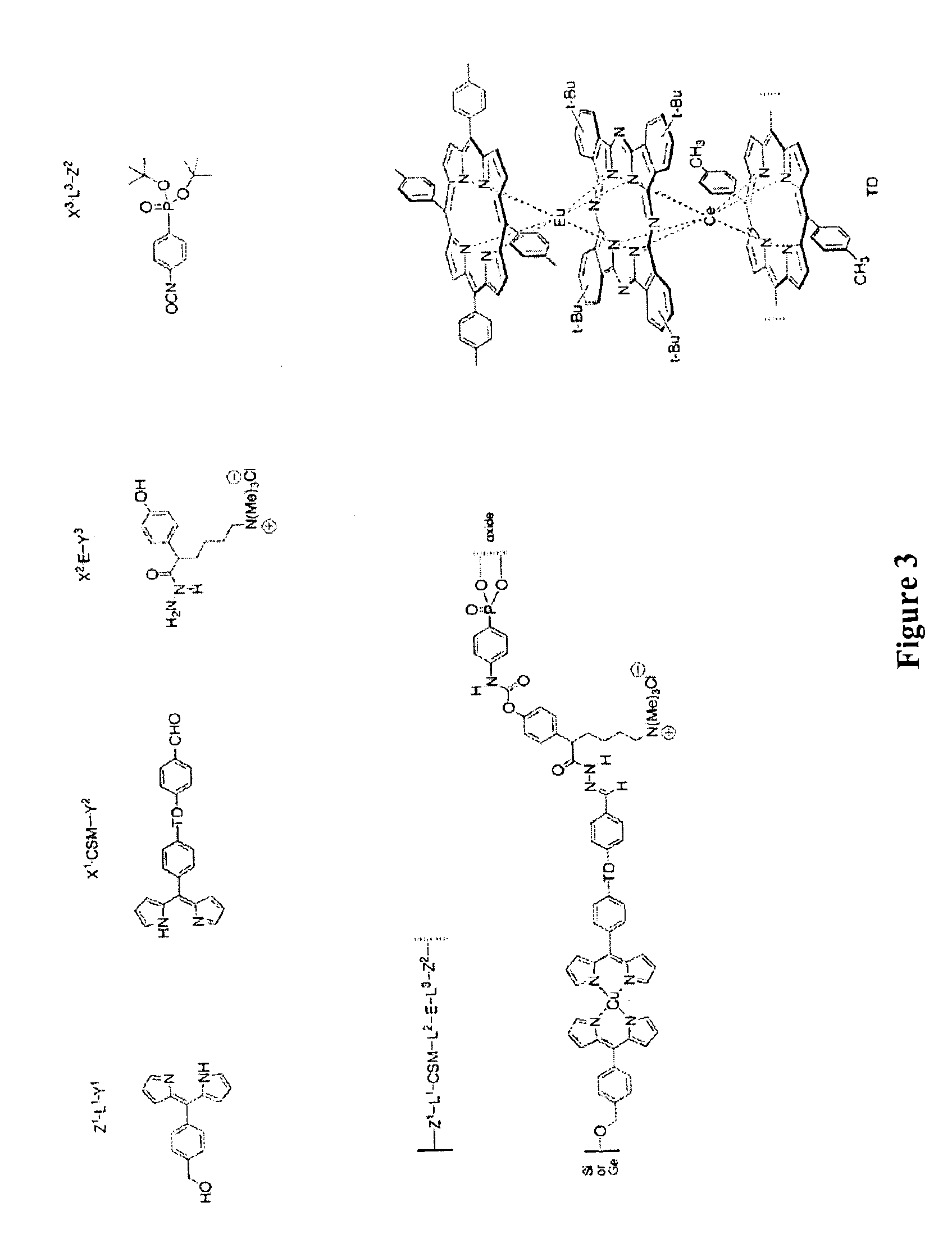
[0016]“Coupling” as used herein refers to the coupling of one molecule to another by one or more strong bonds, such as covalent bonds or electrostatic bonds. Coupling steps may be direct or indirect (e.g., coupling through an intervening molecule such as a photocleavable linking group, additional linking group, etc.).

[0017]“Substrate” as used herein means any substrate, including but not limited to organic and inorganic solid substrates such as glass, silicon, silicon dioxide, etc., which may be insulators, conductors, etc.

[0018]“Charge storage molecule” and “storage molecule” are used interchangeably herein and refer to a molecule having one or more oxidation states that can be used for the storage of information (e.g. a molecule comprising one or more redox-active subunits). Preferred storage molecules have two or more different and distinguishable non-neutral oxidation states. Such charge storage molecules generally comprise a backbone polymer.

[0019]“Charge storage group” as used...


PUM

PropertyMeasurementUnit
temperatureaaaaaaaaaa
voltageaaaaaaaaaa
voltageaaaaaaaaaa

Abstract

A photolithographic method of making an information storage device having different storage characteristics at a plurality of discrete memory locations thereon, comprises the steps of: (a) providing a substrate having a surface portion, said surface portion having a linking group coupled thereto or charge storage group coupled thereto, said linking group or charge storage group having a photocleavable protecting group thereon; (b) exposing at least one first discrete segment of said surface portion to radiant energy sufficient to cleave said protecting group from said linking group or charge storage group and generate a deprotected group, so that said group is deprotected in at least one first discrete memory location and preferably said group remains protected in at least one second discrete memory location. Additional groups are then coupled to the deprotected group as desired. Products produced by such methods are also described.

Description

FIELD OF THE INVENTION[0001]The present invention generally concerns methods for the production of molecular memory devices, and the memory devices so made.BACKGROUND OF THE INVENTION[0002]General challenges in fabricating a hybrid chip containing molecular materials for information storage are that (1) the charge-storage molecule must be attached to an electroactive surface, (2) the electrolyte must be present in the same location as the charge-storage molecule but not elsewhere, (3) the counterelectrode must be located at a controlled distance from the charge-storage molecules. Particularly pressing problems are that often the methods for attachment of molecules to surfaces require very high concentrations, high temperature, and / or the use of reactive intermediates [Cleland, G. et al., J. Chem. Soc. Faraday Trans. 1995, 91, 4001-4003; Buriak, J. M. Chem. Commun. 1999, 1051-1060; Linford, M. R. et al., J. Am. Chem. Soc. 1995, 117, 3145-3155; Hamers, R. J. et al., Am. Chem. Res. 200...

Claims


Application Information

Patent Timeline
Patent Type & Authority Patents(United States)
IPC IPC(8): G11C13/02G03C5/00G03F7/00G11C11/00H01LH01L51/00
CPCH01L51/0089Y10S430/145Y10S430/167Y10S430/143H10K85/351
Inventor LINDSEY, JONATHAN S.
Owner NORTH CAROLINA STATE UNIV
Why Eureka
Try Eureka