

Flat panel display device having planar field emission source
a technology of emission source and display device, which is applied in the direction of instruments, tubes with screens, discharge tubes, etc., can solve the problems that the cathode ray tube cannot be easily adapted for a large-sized display and is still difficult to realize a large-sized display, and achieve the effect of large-sized display
- Summary
- Abstract
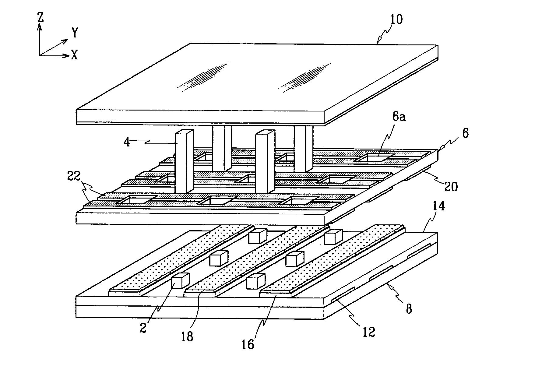
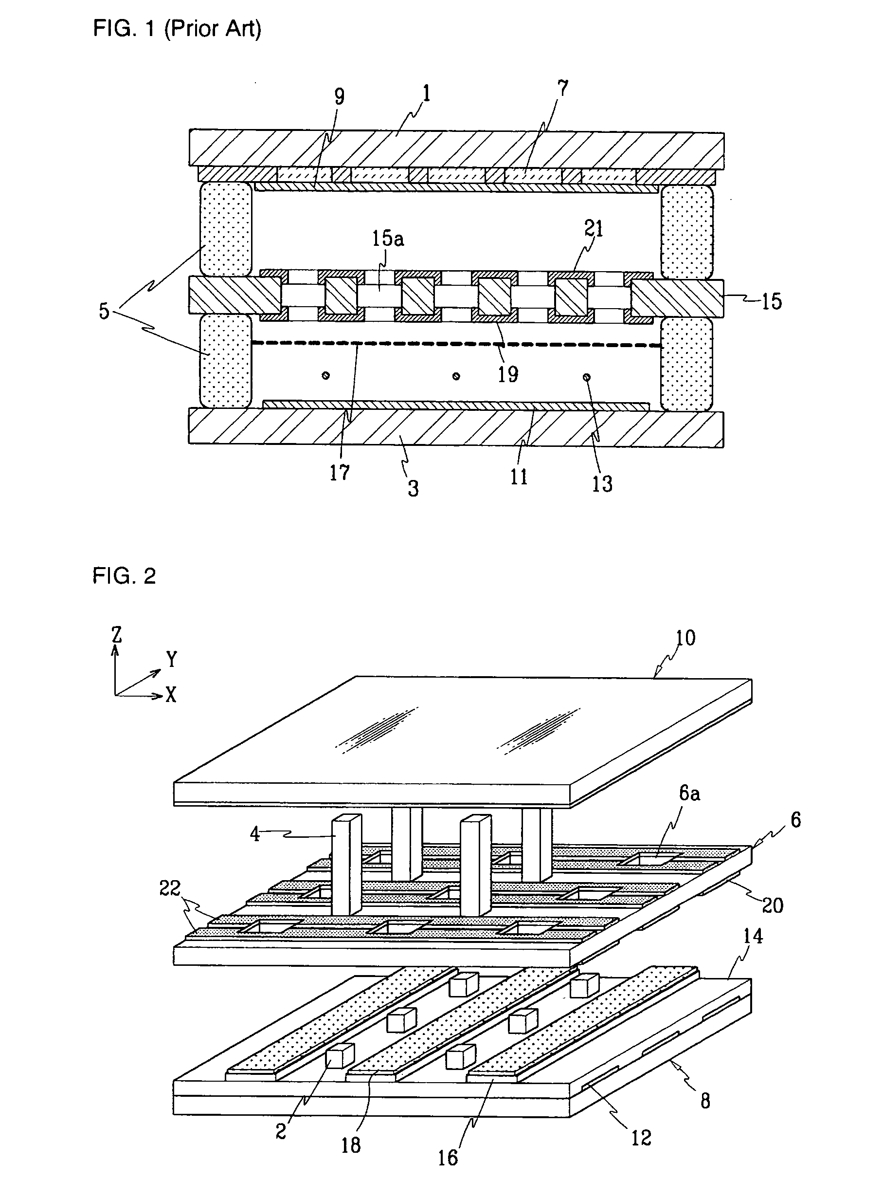
- Description
- Claims
- Application Information
AI Technical Summary
Benefits of technology
Problems solved by technology
Method used
Image

Examples
first embodiment
[0052]A first driving method of the flat panel display according to the present invention is now described with reference to FIG. 5.
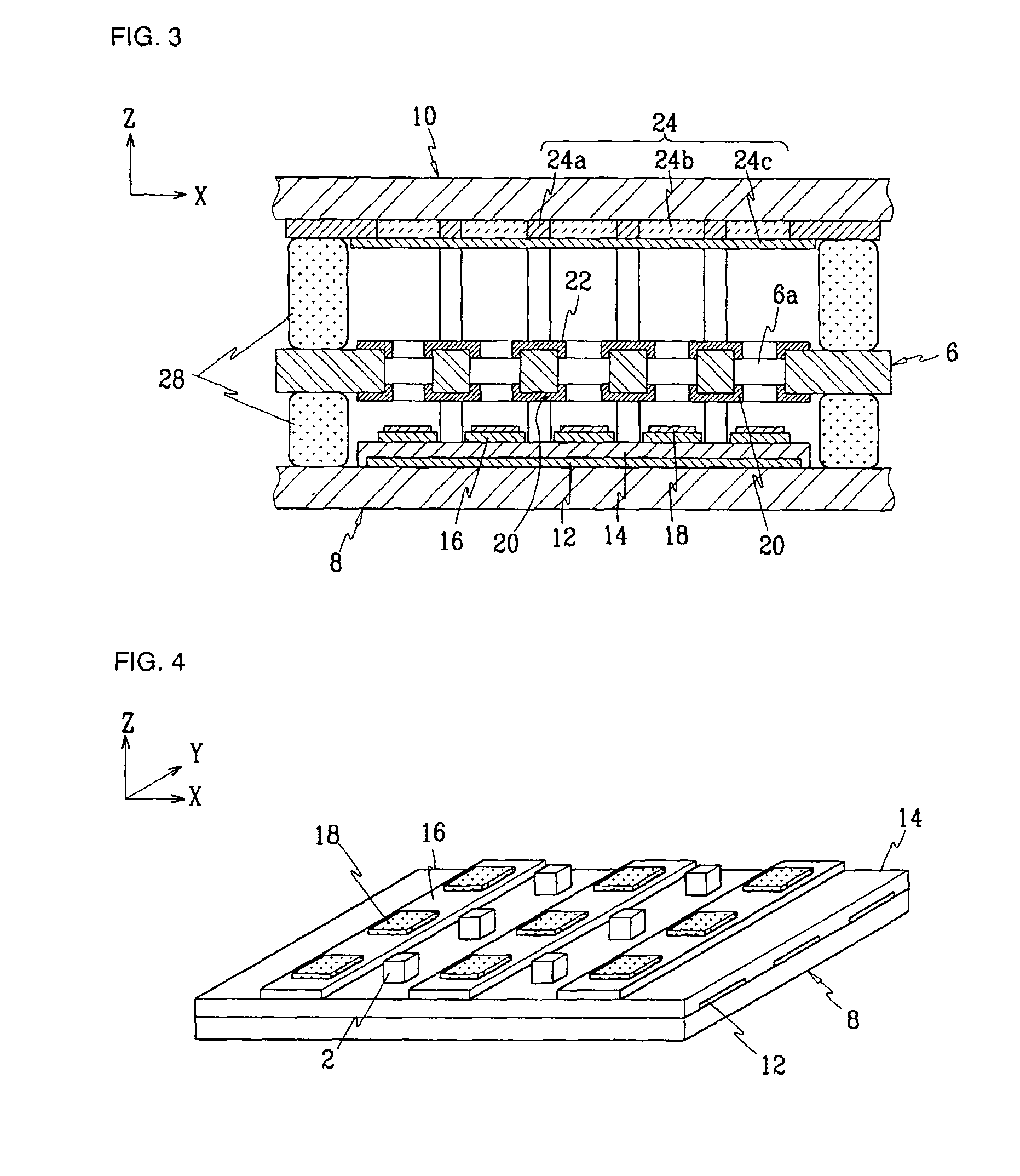
[0053]Scan and data signal voltages are applied to the cathode electrode 16 and the gate electrode 12, respectively, to form an electric field around the emitter 18. The electric field emits electrons from the emitter 18. A focus signal voltage is applied to the first grid electrode 20 to convergence the electrons to the apertures 6a of the grid plate 6. A deflection signal voltage is applied to the second grid electrode 22 so as to deflect the electrons passing through the apertures 6a to corresponding target phosphors. An anode signal voltage is applied to the metal film 24c to accelerate the electrons to the screen 24.
[0054]More in detail, to turn on a specific pixel, when a data signal voltage of +70V and a scan signal voltage of −70V are respectively applied to the gate electrode 12 and the cathode electrode 16, electrons are emitted from the emitt...
second embodiment
[0074]A third driving method on the basis of the above described second embodiment flat panel display is now described.
[0075]Scan and data signal voltages are applied to the cathode electrode 16 and the first electrode 20, respectively. Thus, electrons are emitted from the emitter 18 by an electric field generated around the emitter 18. Then, a field enhancing signal voltage is applied to the gate electrode 12, and a focus signal voltage is applied to the second grid electrode 34 so as to converge electrons at the apertures 6a of the grid plate 6. An anode signal voltage is applied to the metal film to accelerate the electrons toward the screen 24.
[0076]For example, the driving voltages applied to the first grid electrode 20 and the cathode electrode 16 and the field enhancing voltage applied to the gate electrode 12 are identical to those in the above described embodiments. However, a focus signal voltage of about +300V may be applied to the second grid electrode 34.
[0077]By the fo...
third embodiment
[0081]A fourth driving method using the above described third embodiment flat panel display is now described.
[0082]Scan and data signal voltages are applied to a cathode electrode 16 and a gate electrode 12, respectively. Thus, electrons are emitted from the emitter 18. A focus signal voltage is applied to the mesh electrode 36 so as to converge electrons at the apertures 36a of the mesh electrode 36. An anode signal voltage is applied to the metal film 24c to accelerate the electrons toward a screen 24. At this point, a focus signal voltage of +100 may be applied to the mesh electrode 36.
[0083]By the focusing operation of the mesh electrode 36, the electrons can be converged and precisely land on the corresponding target phosphors.
[0084]FIG. 12 shows a flat panel display according to a fourth preferred embodiment of the present invention.
[0085]In this embodiment, a cathode electrode 16 is formed on a surface of the back plate 8 facing the grid plate 6, the cathode electrode 16 havi...
PUM
 Abstract
Description
Claims
Application Information