Apparatus and method for determining voltage using optical observation

a technology of optical observation and apparatus, applied in the direction of electronic circuit testing, measurement devices, instruments, etc., can solve the problems of light emission, high nonlinear emission, and failure of locating semiconductor devices, and achieve the effect of easy detection

Inactive Publication Date: 2006-03-14
CREDENCE INC +1
View PDF25 Cites 27 Cited by
  • Summary
  • Abstract
  • Description
  • Claims
  • Application Information

AI Technical Summary

Problems solved by technology

For example, avalanche breakdown in insulators causes light emission, and detection of such light emission can point to the locations of failure in the device.
Various emission microscopes have been used for detecting locations on the device where the electrical current drawn exceeds the expected levels and therefore could lead to locating failures in semiconductor devices.
In particular, the emission is highly nonlinear in the voltage Vd and is not generally useful for obtaining quantitative voltage information.
Additionally, as is well known, since the current drawn by the device of interest is very small, the emission of the switching device is very faint, requiring single photon detection technology and repeated measurement for obtaining accurate timing of the emission.

Method used


Image

  • Apparatus and method for determining voltage using optical observation
  • Apparatus and method for determining voltage using optical observation
  • Apparatus and method for determining voltage using optical observation

Examples


Embodiment Construction

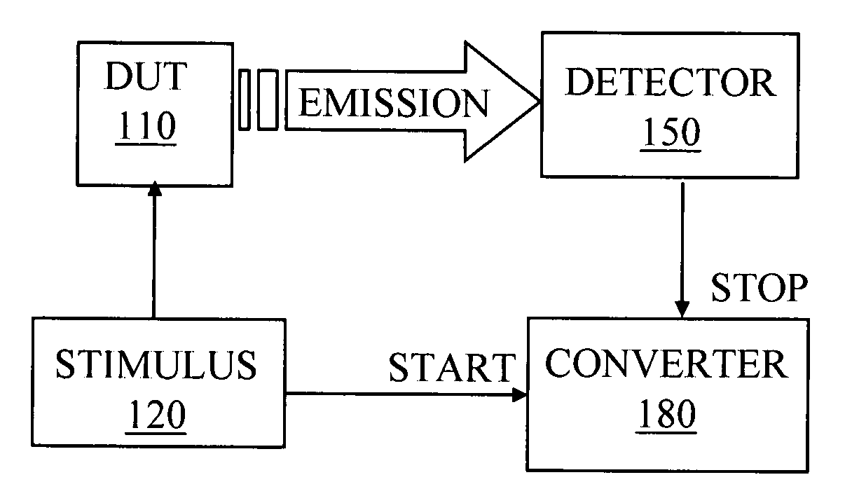
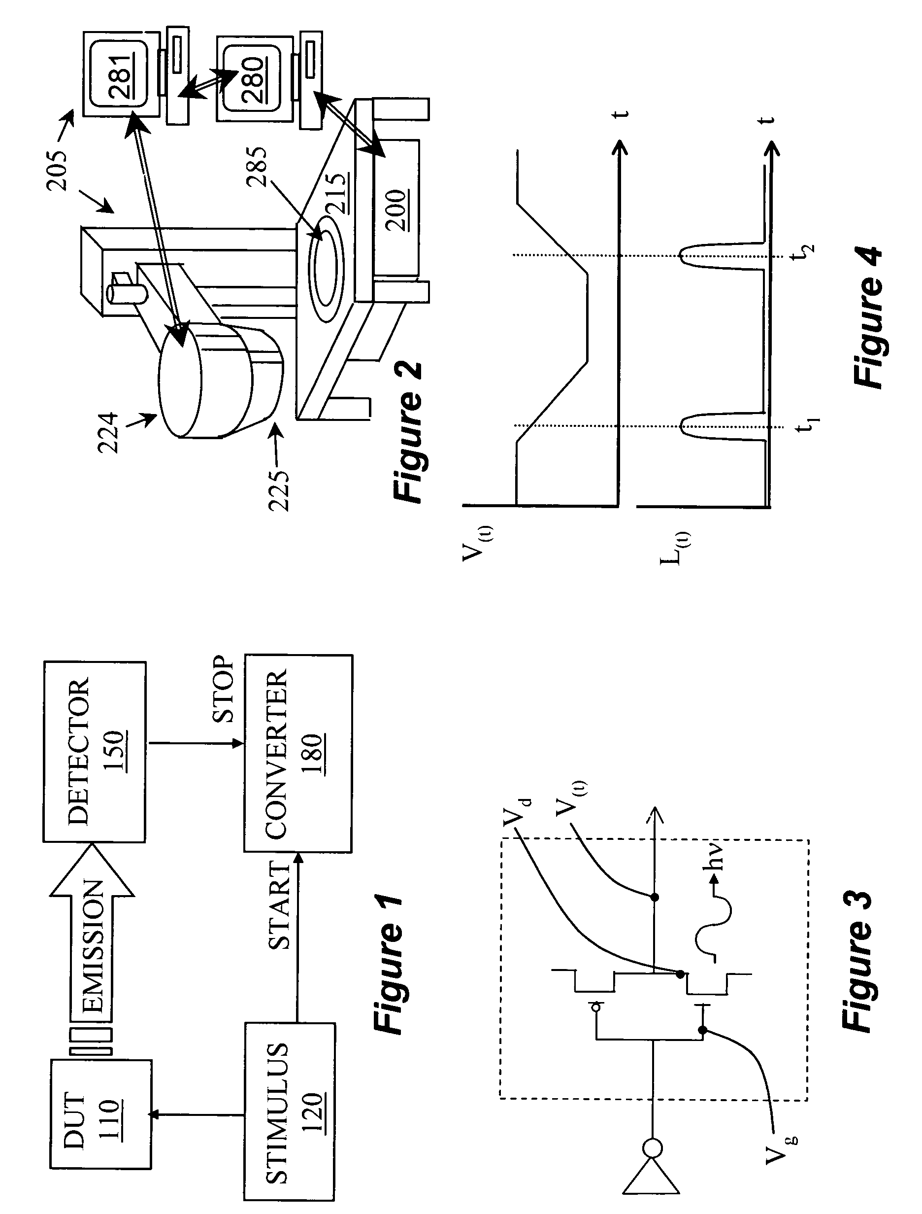
[0037]The present invention provides a testing and debug system particularly suitable for rise time, timing, logic fault localization, and other testing of microchips. The investigation is performed with respect to a time correlation to electrical stimulus provided to the DUT, by detecting light emitted from a specially designed beacon circuit. The beacon circuit is connected to, or fabricated integrally with the DUT.

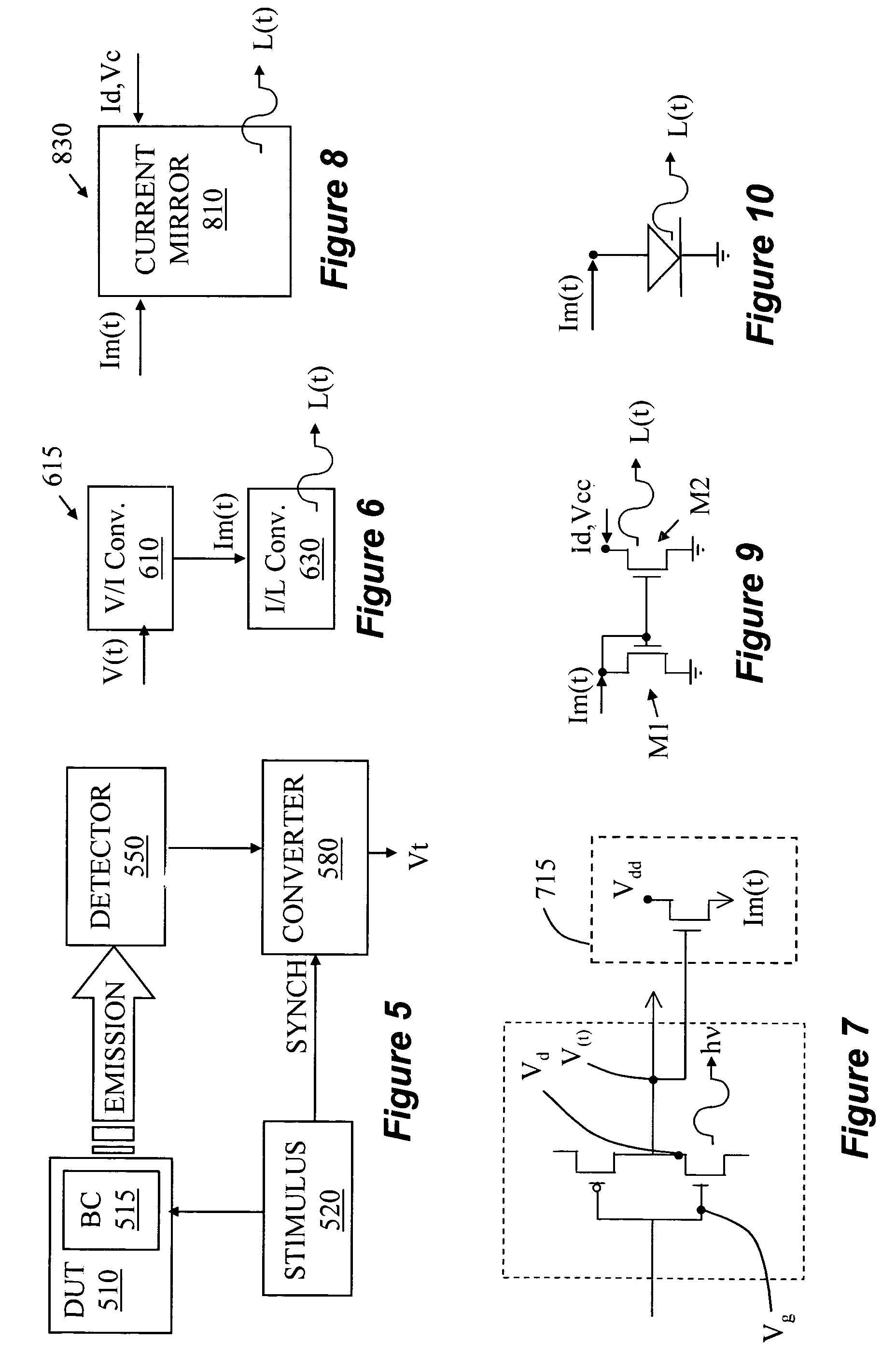
[0038]FIG. 5 is a block diagram depicting the major components of the system according to an embodiment of the invention. As shown, beacon circuit 515 is fabricated within DUT 510, and is connected to a node of interest within the DUT (see, e.g., FIG. 7). The DUT 510 is stimulated, 520, by, e.g., an ATE shown in FIG. 2, that also provides a synch Signal to converter 580. When DUT 510 is stimulated, beacon circuit 515 emits light, which is collected and detected by detector 550. The signal from the detector 580 is input to converter 580, which manipulates the signal to p...


PUM


Abstract

A beacon circuit enabling study of active elements in an integrated circuit is disclosed. The beacon circuit may be integral to a DUT to be tested. The DUT is stimulated by a conventional ATE, so that its active devices are operating. The signal from the active device is sent to the beacon circuit which, in response to the signal, emits light having intensity that is proportional to the value of the signal. In one example, the beacon circuit is constructed as a voltage to current converter having its input connected to the node of interest and its output connected to a current to light converter. In one example, the current to light converter is implemented as a current mirror circuit. One beneficial implementation disclosed is the use of the beacon circuit for the study of voltage supply disturbances.

Description

CROSS REFERENCE TO RELATED APPLICATIONS[0001]This Application claims priority from U.S. Provisional Application Ser. No. 60 / 543,003, filed Feb. 10, 2004, which is incorporated herein by reference in its entirety.BACKGROUND OF THE INVENTION[0002]1. Field of the Invention[0003]The present invention relates to an apparatus and method for determining time-resolved voltage at a node in an integrated circuit using optical observation.[0004]2. Description of the Related Art[0005]It is known in the prior art that various mechanisms in semiconductor devices can cause light emission. Detection of such light emission has been used to investigate semiconductor devices. For example, avalanche breakdown in insulators causes light emission, and detection of such light emission can point to the locations of failure in the device. Similar detection can be used to characterize electrostatic discharge in the device. In electrically stimulated (active) transistors, accelerated carriers (electrons & hol...

Claims


Application Information

Patent Timeline
Patent Type & Authority Patents(United States)
IPC IPC(8): G08B21/00
CPCG01R31/311
Inventor WOODS, GARY LEONARDKASAPI, STEVEN
Owner CREDENCE INC
Why Eureka
Try Eureka