Check patentability & draft patents in minutes with Patsnap Eureka AI!

Rotating semiconductor processing apparatus

Inactive Publication Date: 2006-03-28
ASM AMERICA INC
View PDF30 Cites 33 Cited by
  • Summary
  • Abstract
  • Description
  • Claims
  • Application Information

AI Technical Summary

Benefits of technology

[0011]Briefly stated, the present invention addresses the needs described above by providing a reactor with rotating components to more evenly distribute temperature and processing gases within a reaction chamber. In accordance with one aspect of the present invention, a semiconductor processing apparatus is provided comprising a support structure for supportin

Problems solved by technology

If the temperature varies across the surface of the wafer, uneven deposition of the reactant gas occurs and the thickness and resistivity will not be uniform.
Non-uniformity of deposited layers also results from an uneven distribution of reactant gases over a wafer.
Similarly, non-uniformity or instability of temperature across a wafer during other thermal treatments can affect the uniformity of resulting structures.

Method used


Image

  • Rotating semiconductor processing apparatus
  • Rotating semiconductor processing apparatus
  • Rotating semiconductor processing apparatus

Examples


Embodiment Construction

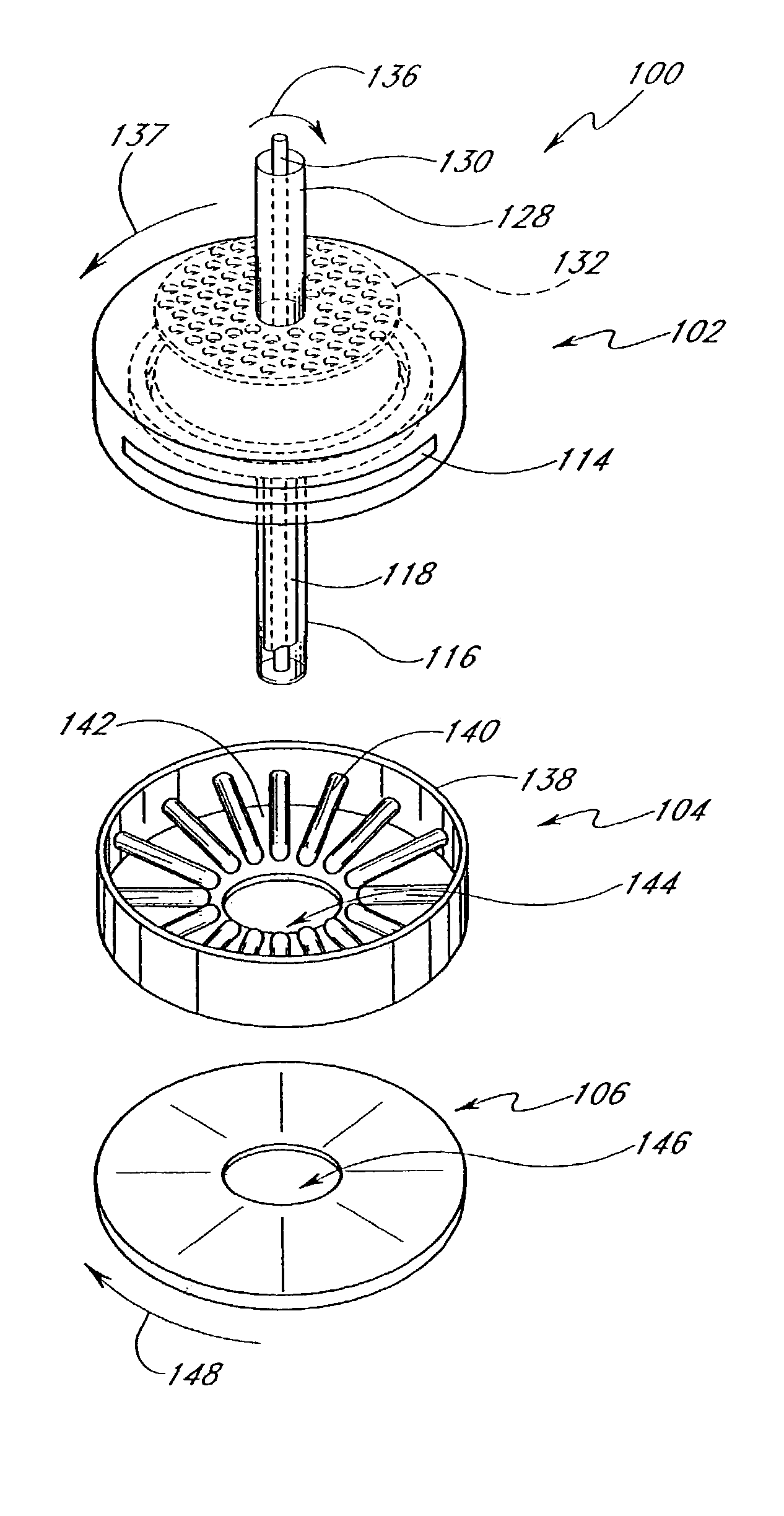
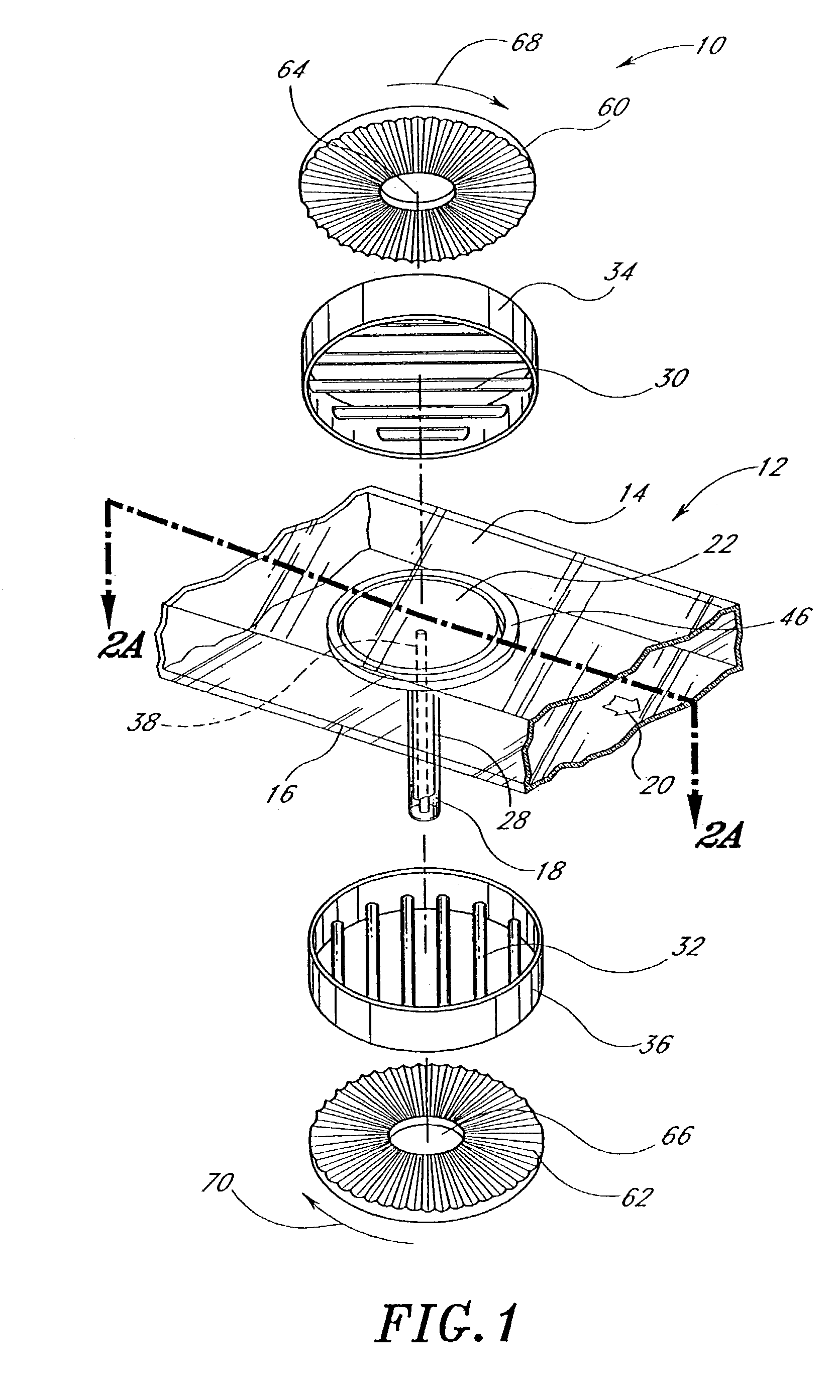
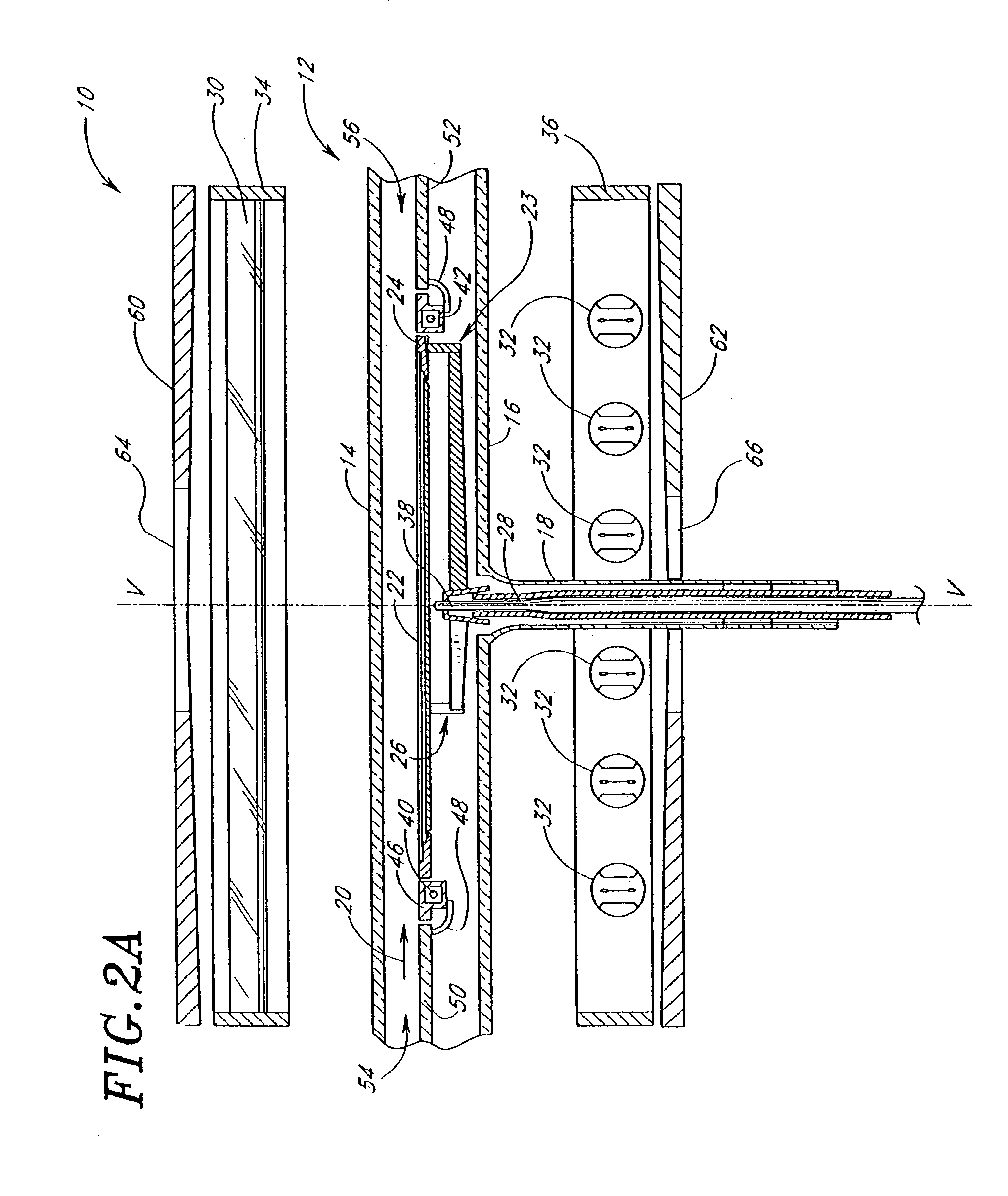
[0024]The embodiments illustrated below describe a portion of an integrated circuit fabrication reactor, more particularly a semiconductor processing chamber having rotating components to improve temperature and gas distribution uńiformity. While the preferred embodiments are described in the context of a “cold wall” CVD reactor for processing semiconductor wafers, it will be understood that the processing apparatus and methods described herein will have utility in the context of reactors of other types. In particular, one of skill in the art can find application for the apparatus and methods described herein for other semiconductor processing equipment, wherein a semiconductor substrate is to be treated at a controlled temperature. The present invention can also be implemented in conjunction with other heating / cooling systems, such as those employing inductive or resistive heating. Moreover, temperature and gas uniformity is often required in the treatment of other substrates, incl...


PUM

PropertyMeasurementUnit
Angular velocityaaaaaaaaaa
Diameteraaaaaaaaaa

Abstract

A reactor for processing semiconductor wafers and the like is provided. The reactor employs one or more rotating components to more evenly distribute temperature or gases within the chamber. In one embodiment, the reactor is provided with rotating reflectors, which reflect the heat generated from radiant heat lamps onto a stationary wafer in a reaction chamber. The rotation of the reflectors provides for a more uniform temperature distribution on the wafer. In another embodiment, the reaction chamber itself is rotated while the wafer is kept stationary. In another embodiment, a rotating showerhead is provided above the wafer through which gases flow to deposit onto the wafer in a uniform manner.

Description

CROSS REFERENCE TO RELATED APPLICATIONS[0001]This is a continuation of U.S. patent application Ser. No. 09 / 550,680 filed on Apr. 17, 2000, now U.S. Pat. No. 6,554,905 which is incorporated herein by reference and made a part of the present disclosure.BACKGROUND OF THE INVENTION[0002]1. Field of the Invention[0003]The present invention relates to an apparatus for processing of semiconductor wafers and the like, and more particularly, to a reactor having rotating components to produce a more uniform deposition.[0004]2. Description of the Related Art[0005]High-temperature ovens, called reactors, are used to create structures of very fine dimensions, such as integrated circuits on semiconductor substrates. One or more substrates, such as silicon wafers, are placed on a wafer support inside the reaction chamber. Both the wafer and support are heated to a desired temperature. In a typical wafer treatment step, reactant gases are passed over the heated wafer, causing the chemical vapor dep...

Claims


Application Information

Patent Timeline
IPC IPC(8): C23C16/00H01L21/00
CPCH01L21/67115Y10T29/41
Inventor GOODWIN, DENNIS L.
Owner ASM AMERICA INC
Features
  • R&D
  • Intellectual Property
  • Life Sciences
  • Materials
  • Tech Scout
  • Unparalleled Data Quality
  • Higher Quality Content
  • 60% Fewer Hallucinations
Learn More