Micromagnetic device for power processing applications and method of manufacture therefor

a micro-magnetic device and power processing technology, applied in the direction of semiconductor/solid-state device details, instruments, soldering apparatus, etc., can solve the problem that the traditional method of rolling and tape winding of thin-film ferromagnetic materials is very costly

Inactive Publication Date: 2006-04-04
BELL SEMICON LLC
View PDF13 Cites 49 Cited by
  • Summary
  • Abstract
  • Description
  • Claims
  • Application Information

AI Technical Summary

Problems solved by technology

Processing thin-film ferromagnetic materials with traditional rolling and tape winding techniques proves to be very costly as the desired tape thicknesses drops below 0.001 inches (i.e., 25 μm).

Method used


Image

  • Micromagnetic device for power processing applications and method of manufacture therefor
  • Micromagnetic device for power processing applications and method of manufacture therefor
  • Micromagnetic device for power processing applications and method of manufacture therefor

Examples


Embodiment Construction

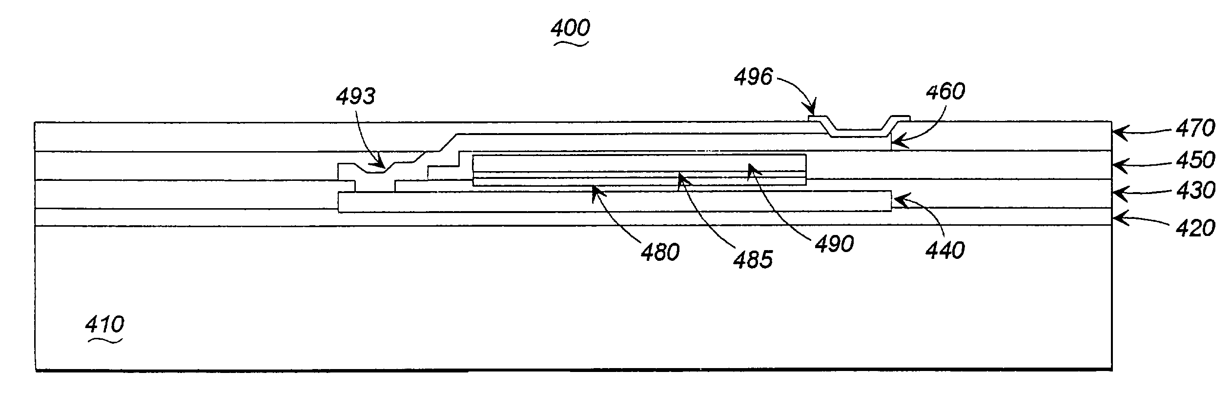
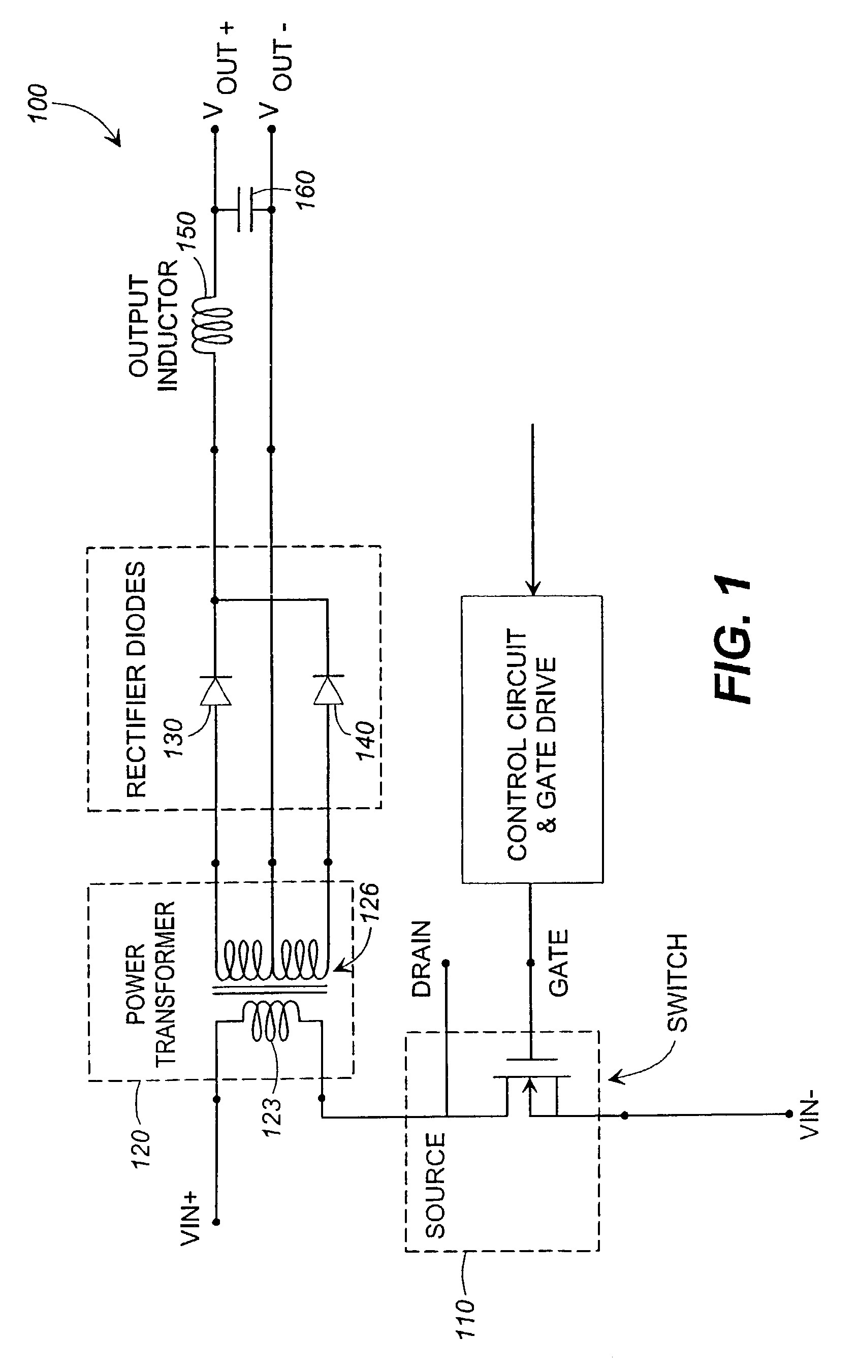
[0019]Referring initially to FIG. 1, illustrated is a schematic diagram of an embodiment of a power processing circuit 100 constructed according to the principles of the present invention. The power processing circuit 100 includes a power train having a conversion stage including a switching circuit 110 for receiving input electrical power VIN and producing therefrom switched electrical power. The power processing circuit 100 further includes a filter circuit (including an output inductor 150 and output capacitor 160) for filtering the switched electrical power to produce output electrical power (represented as a voltage VOUT). The power processing circuit 100 still further includes a power micromagnetic integrated circuit (e.g., transformer) 120, having a primary winding 123 and a secondary winding 126, and a rectifier (including rectifying diodes 130, 140) coupled between the power conversion stage and the filter stage. The transformer 120 is constructed according to the principle...


PUM

PropertyMeasurementUnit
thicknessesaaaaaaaaaa
skin depthaaaaaaaaaa

Abstract

The present invention provides a power micromagnetic integrated circuit having a ferromagnetic core, a method of manufacture therefor and a power processing circuit employing the same, that-includes: (1) a substrate; (2) an insulator coupled to the substrate and (3) a metallic adhesive that forms a bond between the insulator and the ferromagnetic core to secure the ferromagnetic core to the substrate.

Description

[0001]This application is a continuation of currently pending application Ser. No. 09 / 484,498, filed Jan. 18, 2000, Abandoned by Kossives, et al., and entitled “A Micromagnetic Device for Power Processing Applications And Method of Manufacture Therefor.” The application Ser. No. 09 / 484,498 is a divisional of application Ser. No. 08 / 872,250, filed Jun. 10, 1997, which issued on Sep. 12, 2000, as U.S. Pat. No. 6,118,351 to Kossives, et al., and entitled “Micromagnetic Device for Power Processing Applications And Method of Manufacture Therefor.” The above-listed application Ser. No. 09 / 484,498 and U.S. Pat. No. 6,118,351 are commonly assigned with the present invention and are incorporated herein by reference.TECHNICAL FIELD OF THE INVENTION[0002]The present invention is directed, in general, to micromagnetic devices and, more specifically, to a micromagnetic device for power processing applications, a method of manufacture therefor and a power processing circuit employing the same.BAC...

Claims


Application Information

Patent Timeline
Patent Type & Authority Patents(United States)
IPC IPC(8): B23K35/14H01F10/08H01F10/12H01F10/13H01F17/00H01F19/00H01F41/04H01F41/32H01L23/522H01L23/64H01L27/01
CPCH01F17/0006H01F41/046H01L23/5227H01L23/645H01L27/016H01L2924/0002H01L2924/09701H01L2924/3011H01L2924/00H01L21/77
Inventor KOSSIVES, DEAN P.LOTFI, ASHRAF W.SCHNEEMEYER, LYNN F.STEIGERWALD, MICHAEL L.VAN DOVER, R. BRUCE
Owner BELL SEMICON LLC
Why Eureka
Try Eureka