Stacked chip connection using stand off stitch bonding

a stand-off stitch and chip technology, applied in the direction of auxillary welding devices, soldering apparatus, semiconductor/solid-state device details, etc., can solve the problems of direct influence on the location, number, and size of the bond pad

Inactive Publication Date: 2006-04-04
ROUND ROCK RES LLC
View PDF30 Cites 27 Cited by
  • Summary
  • Abstract
  • Description
  • Claims
  • Application Information

AI Technical Summary

Benefits of technology

[0007]Additional features and advantages of the present invention will be more clearly apparent from the detailed description which is provided in connection with accompanying drawings which illustrate exemplary embodiments of the invention.

Problems solved by technology

This downsizing has directly affected the location, number, and size of bond pads for electrical connections for these devices.
However, decreased size and fewer locations of bond pads on various layers of multiple chips presents a different bonding problem.

Method used


Image

  • Stacked chip connection using stand off stitch bonding
  • Stacked chip connection using stand off stitch bonding
  • Stacked chip connection using stand off stitch bonding

Examples


Embodiment Construction

[0017]In the following detailed description, reference is made to various specific embodiments in which the invention may be practiced. These embodiments are described with sufficient detail to enable those skilled in the art to practice the invention, and it is to be understood that other embodiments may be employed, and that structural and procedural changes may be made without departing from the spirit or scope of the present invention.

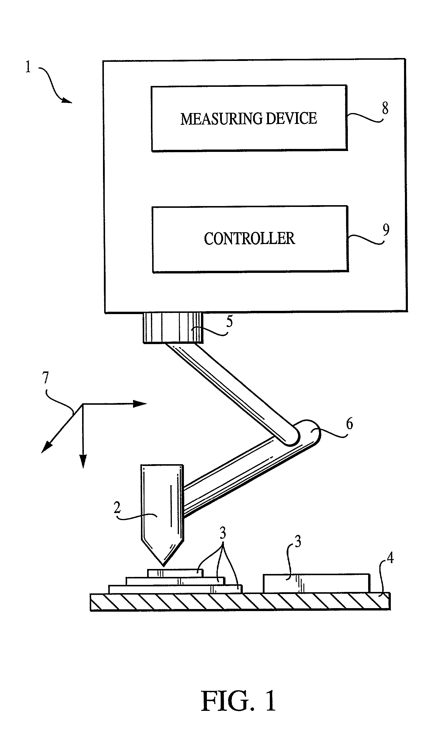
[0018]Before discussing the invention in detail some conventional wire bonding techniques will be discussed with reference to FIGS. 1–4B. Referring now to the drawings, where like elements are designated by like reference numerals, FIG. 1 depicts a wire bonding apparatus generally designated by numeral 1. The wire bonding apparatus may have a wire bonding device 2, such as a capillary, which is controllably positioned relative to workpieces 3 on top of a support surface 4. The bonding device 2 is capable of forming wire bonds at a plurality of bond...


PUM

PropertyMeasurementUnit
bonding areaaaaaaaaaaa
structureaaaaaaaaaa
angleaaaaaaaaaa

Abstract

The present invention provides a structure, apparatus, and method for wire bonding in which a first wire bond is formed between first and second components, a second wire bond is formed between the second component and a third component such that the second wire bond is in electrical communication with the first wire bond, wherein the first and second wire bonds are connected to said first and second components, respectively, using ball bonding.

Description

FIELD OF THE INVENTION[0001]The present invention relates generally to wire bonding, and more particularly, to a method and apparatus for wire bonding multiple semiconductor integrated circuit chips.BACKGROUND OF THE INVENTION[0002]The continuing trend in the semiconductor and integrated circuit industries is to develop and manufacture smaller components. This trend has resulted in integrated circuits and semiconductor devices having higher density due to an increased number of components coexisting in smaller physical areas. This downsizing has directly affected the location, number, and size of bond pads for electrical connections for these devices.[0003]Wire bonding techniques have been developed to accommodate smaller bond pad sizes as well as the stacking of multiple chips in an integrated circuit package. However, decreased size and fewer locations of bond pads on various layers of multiple chips presents a different bonding problem. There exists a need, therefore, for a relia...

Claims


Application Information

Patent Timeline
Patent Type & Authority Patents(United States)
IPC IPC(8): B23K31/00B23K31/02B23K20/00H01L21/607H01L21/98H01L25/065
CPCB23K20/007H01L24/48H01L24/49H01L24/83H01L24/85H01L25/0657H01L25/50H01L24/32H01L24/45H01L24/78H01L2224/32145H01L2224/45144H01L2224/48091H01L2224/48137H01L2224/48145H01L2224/48147H01L2224/48175H01L2224/48471H01L2224/48472H01L2224/48475H01L2224/48599H01L2224/4911H01L2224/49171H01L2224/49175H01L2224/78301H01L2224/8319H01L2224/8385H01L2224/85045H01L2224/85051H01L2224/85205H01L2225/06506H01L2225/0651H01L2924/01079H01L2924/07802H01L2924/14H01L2924/01033H01L2924/00014H01L2924/00H01L2224/05554H01L2224/789H01L2224/85399H01L2224/05599
Inventor BOWEN, NEAL M.
Owner ROUND ROCK RES LLC
Why Eureka
Try Eureka